
Transmission Electron Microscope and Scanning Electron Microscopes
The research activities of the Corrosion and Mechanics of Materials Section are supported by complete metallography/sample preparation rooms equipped with several optical and electron microscopes: a Transmission Electron Microscope and two Scanning Electron Microscopes.
Transmission electron microscope (TEM)

Figure 1: Detail of JEOL 100CXII TEM. Click on image to view larger image.
Transmission electron microscopy is a powerful tool to
investigate crystallographic defects down to the
nanoscale, and is a critical technique to study
irradiated materials. The JEOL 100CXII, a 100kV TEM with a lattice resolution of 0.2 nm, is dedicated for
microstructure observations on high-dose
neutron-irradiated specimens. The work focuses on
defect structure and microstructure evaluations. The
examinations help understand various degradation
mechanisms related to neutron irradiation.
Scanning electron microscopes (SEMs)
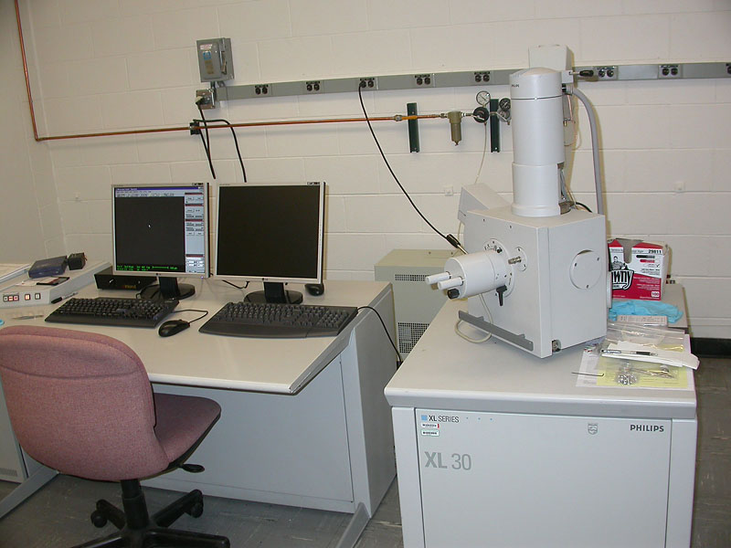
Figure 2: Philips XL30 SEM. Click on image to view larger image.
Scanning
electron microscopy is the most powerful technique for
surface characterization and quantitative analysis on
corrosion and mechanical tested specimens. Two SEMs
are currently available for various research programs
in the section. One is a Jeol JSM 6400 SEM which has a
resolution of 3.5 nm (at 35 KV- 8 mm WD) and is
equipped with PGT image and EDS acquisition systems.
This SEM is used as a general purpose microscope for
non-irradiated specimens. The second SEM is Philips
XL30 which has a resolution of 2.5nm at 30kV nm, and
is equipped with an EDAX EDS system. This microscope
is dedicated for the examination examining radioactive
specimens, and the column and operator desk are
installed approximately 1ft. apart to allow for a lead
shield to be installed around the column. This SEM has
two control consoles, one of which will be installed
outside the room allowing for remote operation.
Last Modified: Tue, April 19, 2016 5:18 AM