

Integration Lab
Contacts
- Integration Lab Manager
- John Nogan
- Sandia National Laboratory
- Process Technologist
- Denise B. Webb
- Sandia National Laboratory
- Equipment Technologist
- Joseph Lucero
- Sandia National Laboratory
- CINT Technician/E-beam writer
- Tony James
- Sandia National Laboratory
- General Technologist
- Bill Ross
- Sandia National Laboratory
Integration Laboratory Capabilities
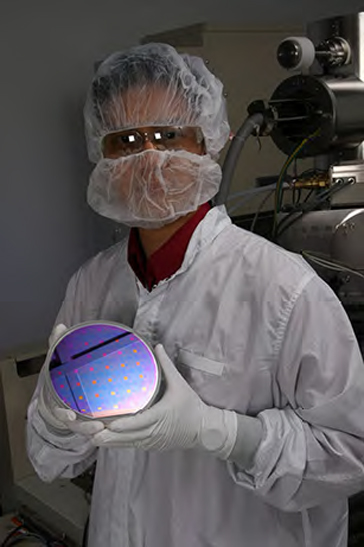
The Integration Lab allows CINT staff and users to integrate nano-enabled components using up to 100 mm wafer processing technology. Capabilities include five generic processing areas: Contact Lithography, Plasma Systems, Wet Processes, Physical Vapor Deposition, and Thermal Processes. In this facility CINT staff and users can work with samples as large as 100mm and as small as 20nm. For more information, please see the Tool Sets list.
Tool Sets
The facility tool sets range from plasma deposition and etching to focused ion beam nano-fabrication. The Integration Laboratory is staffed by a team of process engineers with over 60 years of combined micro-processing experience. Access to the Integration Laboratory tool sets is obtained via the CINT user program.
Lab Staffing
Feasibility questions should be directed to the Integration Lab Manager, John Nogan.
Training Requirement
As with all approved CINT user projects, users conducting work in the Integration Laboratory are required to successfully complete the appropriate training for their project. Please contact the Integration Lab Manager, John Nogan, for more information.