
Official websites use .gov
A .gov website belongs to an official government organization in the United States.
Secure .gov websites use HTTPS
A lock (
) or https:// means you've safely connected to the .gov website. Share sensitive information only on official, secure websites.
Nanolithography Design Tools
Accurate production of nanoscale features on semiconductor chips is essential to their performance, but typical design tools cater to the dominance of straight lines and right angles in traditional chips, not the curved features needed for new device designs. Researchers at NIST created new software to help chip designers create smooth, complex curves, enabling the development of new kinds of semiconductor chips.
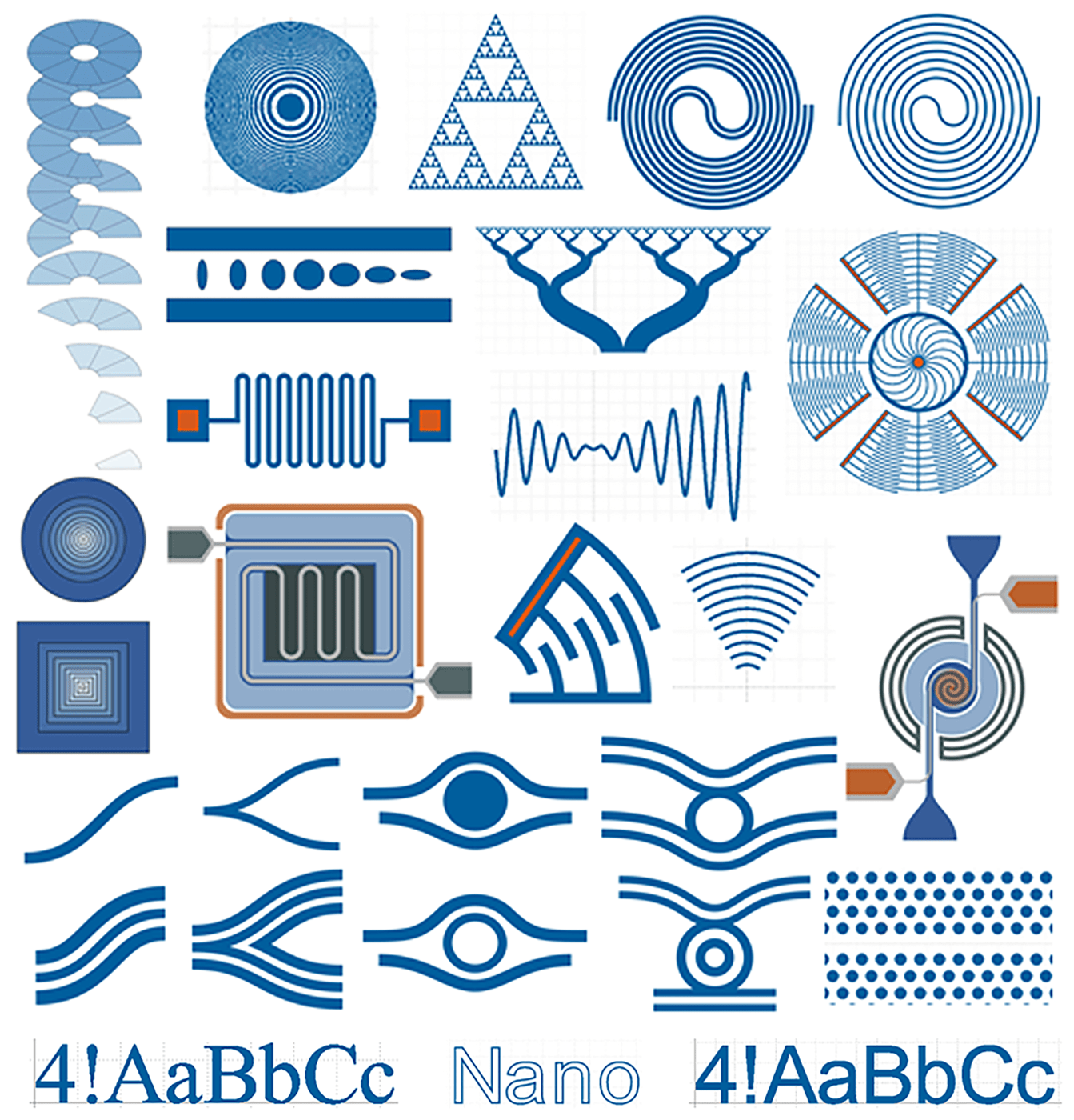
Overcoming a major hurdle in producing new types of nanoscale devices, experts at NIST created the Nanolithography Toolbox, a software package that allows users to produce smooth, complexly curved designs in a standard file format. Researchers use these designs in new devices that have unique mechanical properties and guide light in new ways. The toolbox has been downloaded more than 1,300 times.
Nanolithography techniques carve away tiny amounts of material, layer by layer, to create special designs with highly tuned properties. Existing software packages, optimized for traditional electronic circuits, produce designs with straight lines and right angles. Attempting to create curves for other kinds of devices can result in features with jagged edges, which significantly affects performance.
To solve this design problem, NIST scientists developed a computer-aided design (CAD) software package for scripting and streaming complex shapes to a file format most nanolithography tools use. The Nanolithography Toolbox uses the freely available, Java-based (JGDS) library for encoding shapes to GDSII objects. It runs on Linux, Windows and MacOS, and is free for users to download from the NIST website.