2010
Quantitative and Depth-Resolved Investigation of Deep-Level Defects in InGaN/GaN Heterostructures
December 24, 2010
Journal of Electronic Materials recently published the article “Quantitative and Depth-Resolved Investigation of Deep-Level Defects in InGaN/GaN Heterostructures” authored by EFRC scientists Andy Armstrong, Mary Crawford, and Daniel Koleske. Deep-Level Optical Spectroscopy (DLOS) was used to obtain depth-resolved defect energy levels through the active region (i.e., both quantum wells and quantum barriers) in InGaN multiquantum-well structures.
Abstract: Deep-level defects in In0.17Ga0.83N/In0.02Ga0.98N/p-GaN:Mg heterostructures were studied using deep-level optical spectroscopy (DLOS). Depth-resolved DLOS was achieved by exploiting the polarization-induced electric fields to discriminate among defects located in the In0.17Ga0.83N and the In0.02Ga0.98N regions. Growth conditions for the In x Ga1−x N layers were nominally the same as those in InGaN/GaN multi-quantum-well (MQW) structures, so the defect states reported here are expected to be active in MQW regions. Thus, this work provides important insight into defects that are likely to influence MQW radiative efficiency. In0.17Ga0.83N-related bandgap states were observed at E v + 1.60 eV and E v + 2.59 eV, where E v is the valence-band maximum, compared with levels at E v + 1.85 eV, E v + 2.51 eV, and E v + 3.30 eV in the In0.02Ga0.98N region. A lighted capacitance–voltage technique was used to determine the areal density of deep states. The possible origins of the associated defects are considered along with their potential roles in light-emitting diodes.
EFRC Lunch Celebration & Ken Lyo Retirement
December 14 & 16, 2010


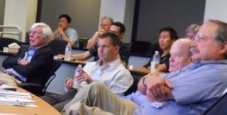
Thirty-one EFRC staff, post-docs, students and support staff celebrated our first full calendar year of work under the EFRC with a December 14 lunch at Scalo’s restaurant in Albuquerque. The lunch was an opportunity to gather informally and discuss highlights of research from the past year, and to plan for the coming year. At the lunch, Jerry Simmons, Director of the EFRC, presented attendees with coffee cups that he designed, embossed with the EFRC logo.
A couple of days later, at our December 16 SSLS coffee/dessert hour, we had a short farewell gathering for EFRC staff member Ken Lyo. After a long career at Sandia National Laboratories, working largely in the area of excitation, transport and relaxation of electronic excitations in condensed matter and semiconductor systems, Ken retired on December 23. Ken’s most recent work, supported by the EFRC, was in the area of energy transfer between semiconductor nanostructures (quantum wells, wires and dots) containing exciton and electron-hole plasma excitations.
Presentation to the New Mexico Energy Efficiency Working Group
December 13, 2010

Jerry Simmons (EFRC Director) and Mike Coltrin (EFRC Co-Director) gave the feature presentation at the inaugural meeting of the New Mexico Energy Efficiency Working Group of the state’s Energy Conservation and Management Division.
Their talk, “Solid-State Lighting: a New, Green Technology,” provided an introduction to the various lighting technologies in use today, and the energy-savings and advanced features that are possible with the use of solid-state lighting. The working group’s purpose is to exchange information among practitioners about trends and activities, whether they are related to technology, policies or practices. Other speakers at this initial meeting discussed the adoption of an updated building code and the status of energy efficiency projects funded by the Recovery Act.
Energetics of Lanthanum Tantalate Materials
November 30, 2010

In state-of-the-art warm-white LEDs, blue light from an LED is color-mixed with green and red light emitted from blue-LED-pumped phosphors. The red phosphor, however, typically has a fairly broad (150 nm FWHM) emission. The result is wavelength spillover into the deep red where the human eye is insensitive, and a decrease in spectral efficiency.
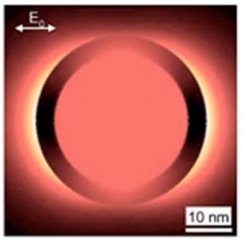
Recently, EFRC scientists May Nyman, Lauren Shea-Rohwer and Jim Martin, and Sandia scientists Mark Rodriguez and Paula Provencio developed a novel red phosphor based on pyrochlore-type rare earth tantalates doped with europium. The new phosphor: (a) has a very narrow emission in the wavelength range (610-620 nm) considered ideal for solid-state lighting, (b) can be directly excited by blue light, (c) is efficient, having quantum yields as high as 78%, even at an early stage of development, (d) can be synthesized in a nanoparticle microstructure for reduced optical scattering, and (e) is extremely chemically and electrochemically stable.
Pyrochlore-type rare earth tantalates have the nominal stoichiometry A2Ta2O7, where A is usually a rare or alkaline earth metal in an eight-coordinate site, and the Ta transition metal sits in a six-coordinate site. Previously, rare-earth tantalates had been limited to synthesis through high temperature, solid-state processes – processes in which atomic transport is inherently short-range and hence incompatible with the exploration of pure phases with compositions different from that of the parent phase. Thus, a new aqueous synthetic route had first to be developed, one that bypassed a fundamental incompatibility between the solubilities of the two usual starting oxides: tantalum oxides are base-soluble, while rare-earth oxides are acid-soluble. The result was a hydrothermal synthesis route that (a) begins with the water-soluble K+-salt of the [Ta6O19]8- polyoxometalate ion and base-soluble lanthanide citrate complexes, (b) proceeds through various intermediate phases (Ln2Ta2O7(OH)2 and KLnTa2O7), (c) enroute to stabler final phases formed upon annealing at high temperatures.
In order to better understand how to control this new but also complex synthesis process, UC Davis scientists Toni Forbes and Alexandra Navrotsky, in collaboration with EFRC scientist May Nyman and Sandia scientist Mark Rodriguez, studied the relative energetics of the various phases using high-temperature oxide melt solution calorimetry. Their results were just published in the Journal of Solid State Chemistry, in a paper titled “The energetics of lanthanum tantalate materials.” Among their conclusions are: that the LaTaO4 phase produced upon annealing at 850C is the stablest of the various polymorphs; and that this stability is consistent with maximizing the distance between lanthanum and tantalum cations, thereby minimizing repulsions between them.
Caption: Eu-doped lanthanum tantalate under photographed UV-excitation.
Strain influenced indium composition distribution in GaN/InGaN core-shell nanowires
November 4, 2010

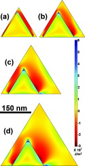
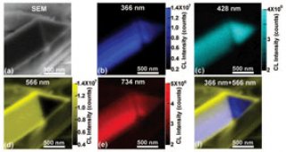
In a recent paper published in Applied Physics Letters, EFRC scientists Qiming Li and George Wang explored the growth of high-Indium-content InGaN on the sidewalls of free-standing facetted GaN nanowires. Not surprisingly, strong segregation effects were observed: the initial InN composition is low (~20%) but increases (to ~40%) as growth progresses. Moreover, strong growth anisotropies were also found: InGaN growth occurred preferentially on a (2201) facet that emerges during growth and anti-preferentially on a (0001) c-plane facet. Most importantly, however, no evidence was found for a breakdown in planar 2D growth on the sidewalls.
These observations are consistent with the idea that some strain is accommodated by macroscopic deformation, facilitated by the small dimensions of the GaN nanowire core. Highly anisotropic growth in one direction enables strain accommodation in perpendicular directions: in this case preferential growth on one sidewall enables strain accommodation in directions parallel to that sidewall. Interestingly, this is an idea often discussed for growth along a nanowire’s longitudinal direction, but these observations indicate that this idea may also apply to growth perpendicular to that direction.
These results indicate that GaN nanowires may offer a route to the wider range of InGaN alloy compositions desirable for visible optoelectronics, including solid-state lighting and photovoltaics.
Caption: (a) SEM image of a GaN/InGaN core-shell nanowire showing inner GaN core and darker InGaN shell. (b)–(e) Monochromatic CL images of the nanowire at 360, 480, 600, and 700 nm. (f) Color composite image of (b)–(e). The scale bar in (a) applies to all images.
Analysis of thermal properties of GaInN light-emitting diodes and laser diodes
October 19, 2010 
EFRC scientists E. Fred Schubert (at our Partner Institution RPI) and his research group recently completed an analysis of heat-transfer processes in LEDs and laser diodes. Their work has been published in a paper titled “Analysis of thermal properties of GaInN light-emitting diodes and laser diodes,”in the Journal of Applied Physics.
Abstract: The thermal properties, including thermal time constants, of GaInN light-emitting diodes (LEDs) and laser diodes (LDs) are analyzed. The thermal properties of unpackaged LED chips are described by a single time constant, that is, the thermal time constant associated with the substrate. For unpackaged LD chips, we introduce a heat-spreading volume. The thermal properties of unpackaged LD chips are described by a single time constant, that is, the thermal time constant associated with the heat spreading volume. Furthermore, we develop a multistage RthCth thermal model for packaged LEDs. The model shows that the transient response of the junction temperature of LEDs can be described by a multiexponential function. Each time constant of this function is approximately the product of a thermal resistance, Rth, and a thermal capacitance, Cth. The transient response of the junction temperature is measured for a high-power flip-chip LED, emitting at 395 nm, by the forward-voltage method. A two stage RthCth model is used to analyze the thermal properties of the packaged LED. Two time constants, 2.72 ms and 18.8 ms are extracted from the junction temperature decay measurement and attributed to the thermal time constant of the LED GaInN/sapphire chip and LED Si submount, respectively.
Strain Influenced Indium Composition distribution in GaN/InGaN core-shell nanowires
October 14, 2010 
Applied Physics Letters recently published the paper “Strain influenced indium composition distribution in GaN/InGaN core-shell nanowires”, by EFRC scientists Qiming Li and George Wang. The paper examined the effect of strain on the incorporation of In into InGaN nanowires.
Abstract: The optical properties, indium concentration and distribution, defect morphology, and strain distribution of GaN/InGaN coaxial nanowires grown by metal organic chemical vapor deposition were investigated using spatially resolved cathodoluminescence, scanning transmission electron microscopy, and finite element analysis. The results indicate that InGaN layers with 40% or greater indium incorporation and low defect density can be achieved. The indium distribution in the InGaN shell layer was measured and qualitatively correlated with the calculated strain distribution. The three-dimensional compliance of the GaN nanowire leads to facile strain relaxation in the InGaN heteroepitaxial layer, enabling high indium incorporation and high crystalline quality.
Carrier recombination mechanisms and efficiency droop in GaInN/GaN light-emitting diodes
September 30, 2010 
EFRC scientists Mary Crawford and Daniel Koleske (Sandia Labs) and Fred Schubert and his research group (RPI) and recently published a paper titled “Carrier recombination mechanisms and efficiency droop in GaInN/GaN light-emitting diodes” in Applied Physics Letters. The team examined the charge-carrier density-dependence of carrier leakage and its potential impact on LED efficiency droop.
Abstract: We model the carrier recombination mechanisms in GaInN/GaN light-emitting diodes as R = An+Bn2+Cn3+f(n), where f(n) represents carrier leakage out of the active region. The term f(n) is expanded into a power series and shown to have higher-than-third-order contributions to the recombination. The total third-order nonradiative coefficient (which may include an f(n) leakage contribution and an Auger contribution) is found to be 8×10⁻²⁹ cm6 s−1. Comparison of the theoretical ABC+f(n) model with experimental data shows that a good fit requires the inclusion of the f(n) term.
Solid-State Lighting “The Case” Ten Year After and Future Prospects
September 28, 2010

Ten years ago, four authors from Hewlett-Packard/Lumileds and Sandia National Laboratories wrote a white paper entitled “The Case for a National Research Program on Semiconductor Lighting.” That paper outlined, for the first time in a comprehensive manner, the promise and potential of semiconductor light-emitting diodes for general illumination. In doing so, the white paper helped trigger enthusiasm and investments in the technology by industries and governments on a global scale.
In an article just published in physica status solidi (a) titled ”Solid-State Lighting: ‘The Case’ Ten Years After and Future Prospects,” two of the original four authors still active in SSL, Roland Haitz (now retired from Hewlett-Packard/Lumileds) and EFRC scientist Jeff Tsao, provide comments on the white paper through the lens of ten years of progress. They discuss trends that the white paper forecast correctly and those that it forecast incorrectly, as well as make a set of new predictions for the coming 10-20 years. Also, the original white paper has been made available archivally for the first time, as supplemental online material to this article.
Caption: This Haitz’ Law figure shows two sets of data: The flux/lamp set describes the highest flux red or cool-white lamp that could be commercially purchased in a given year between 1968 and 2010. The original equipment manufacturers (OEM) cost/lm set describes the lowest costs per lumen for red or cool-white lamps that were commercially offered in a given year between 1973 and 2010. The lamps in the flux/lamp set may or may not be the same lamps entered into the cost/lumen set. The two trend lines are based on red data only, with the white data superimposed on the red trend lines. The different red symbols correspond to the different red materials technologies indicated in the diagonal labels at the bottom of the graph.
Jerry Simmons and Jeff Tsao Give Seminar at the World Bank
September 28, 2010

Jerry Simmons (EFRC Director) and Jeff Tsao (EFRC Chief Scientist) visited the World Bank (Washington DC) on September 28, 2010. They presented a research seminar to the Development Research Group, Environment and Energy Team (DECEE) titled “Lighting Technologies, Costs, and Energy Demand: Global Developments to 2030.” The seminar was based on recent work on the energy economics of solid-state lighting, co-authored by Jeff Tsao, Harry Saunders, Randy Creighton, Mike Coltrin and Jerry Simmons. Jerry and Jeff’s host was Jon Strand, Senior Economist in the Development Research Group, Environment and Energy Team, and also Professor of Economics at the University of Oslo, Norway.
The discussion during and after the talk was lively, and brought out a number of interesting issues. One was that artificial lighting plays an important role in enhancing safety and productivity in the developing world, and solid-state lighting will play an important role in making such lighting more affordable. Another is that solid-state lighting is already making significant inroads into lighting in the developing world. Because of the ubiquity of Nokia cell phones and cell phone chargers, solid-state lights that are battery powered and compatible with these Nokia chargers are becoming increasingly popular.
Jeff and Jerry’s abstract:
Artificial light has long been a significant factor contributing to the quality and productivity of human life; and increasingly so in lower-income countries. Humanity uses huge amounts of energy to produce it. The presenters review possible implications of an emerging technology, solid-state lighting, which promises performance features and efficiencies well beyond those of traditional artificial lighting, for human welfare and energy consumption. They discuss potential consequences of this technology with respect to (a) the global consumption of energy going into lighting up to 2030, and (b) the human productivity and welfare associated with that consumption. They first estimate baseline magnitudes using simple extrapolations of past behavior, and then discuss ways in which the future lighting demand could differ from this baseline. Even if solid-state lighting leads to substantial reductions in unit energy costs of lighting, global electricity consumption for lighting could still increase, due to great expected increases in lighting demand from lower-income countries.
(A video of the full presentation is available for viewing.)
Internal Efficiency of InGaN Light-emmitting Diodes: Beyond a Quasi-equilibrium Model
September 23, 2010

Significant progress has been made in advancing the state-of-the-art in InGaN light-emitting diodes for solid-state lighting. However, performance limitations remain. Among the most important of these are efficiency losses at high current densities (efficiency droop), or at long wavelengths (the green gap), or under adverse operating conditions (e.g., high temperatures). Presently, there is much debate regarding the carrier recombination mechanisms that underlie these efficiency losses. Most attempts to model the relative rates of these mechanisms assume that they are proportional to simple polynomial terms in total carrier density N: a Shockley-Read-Hall defect mechanism AN, a spontaneous emission recombination mechanism BN2, and an Auger or (other higher-order) mechanism CN3. The A, B and C coefficients are used as constant parameters and are typically fit to experimental measurements. Despite its widespread use, this simple “ABC” model is largely inadequate for accurately describing relevant behavior, including carrier recombination in the high carrier density regime.
EFRC scientists Weng Chow, Mary Crawford and Jeff Tsao, along with Michael Kneissl (of the Technische Universitat Berlin) have just published, in Applied Physics Letters, a paper titled “Internal efficiency of InGaN light-emitting diodes: Beyond a quasi-equilibrium model.” In this paper, they describe a more comprehensive model for investigating the different physical mechanisms that may contribute to InGaN LED performance limitations. Central to the model is a more detailed description of carrier relaxation and recombination processes. While still based on rate equations, the rates of the various mechanisms take into account the microscopic electron and hole occupation probabilities of momentum (k) states. This allows band-structure properties to enter directly into the rate equations; allows for a more detailed treatment of carrier-carrier and carrier-phonon scattering; and allows for a more accurate determination of electron and hole distributions (e.g., their temperatures). For example, one key result is that, with increasing current injection and overall carrier densities in InGaN LEDs, electron and hole distributions become hotter, decreasing the effective B coefficient for the spontaneous emission recombination mechanism.
EFRC Participation in International Workshop on Nitride Semiconductors
September 19-24, 2010

EFRC scientists Andy Armstrong, Bob Biefeld, Mike Coltrin, Mary Crawford, post-doc Tania Henry, Normand Modine, George Wang, and Jon Wierer, as well as Sandia scientists Andy Allerman, Steve Lee, and Jeff Nelson, participated in this week’s International Workshop on Nitride Semiconductors (IWN2010) at the Marriott Tampa Waterside Hotel & Marina in Tampa, Florida.
- Jon Wierer gave an invited talk (with co-authors Dan Koleske, Art Fischer, Steve Lee, Greg Nielson and Murat Okandan) on “InGaN-Based Photovoltaic Devices for High-Efficiency Mechanically Stacked Multi-junction Cell Structures.” Jon Wierer also served as chair of a technical session on “Hydrogen Generation and Thermoelectrics.”
- Andy Armstrong gave a talk (with co-authors Andy Allerman and Mary Crawford) on “Effect of growth conditions on defect incorporation and optical efficiency of AlGaN multi-quantum wells.”
- Andy Allerman gave a talk (with co-authors Jon Wierer, Mary Crawford, Qiming Li and Steve Lee) on “Impurity-Induced Disordering in Mg- and Si-doped AlGaN-AlN Superlattices.” In addition, Andy served as chair of the technical session on “Epitaxial Growth of GaN.”
- Steve Lee gave a talk (with co-authors Dan Koleske and Mary Crawford) on “Effect of Non-Ideal Structural Variations on X-ray Diffraction by InGaN/GaN Multiple Quantum Wells.”
- Jeff Nelson served as chair of a technical session on “Nitride Photovoltaics.”
- George Wang gave a talk (with co-author Qiming Li) on “Growth and Laser-free Lift-off of High-quality GaN Films Using Self-assembled Silica Microsphere Monolayers.” George gave a second talk (with co-author Qiming Li) on “Spatially-resolved Investigation of Luminescence and Composition in III-Nitride Nanowires.”
A student of EFRC external partner Professor Jung Han of Yale University, Chris Yerino, gave an invited talk (co-authored by Mike Coltrin) on “GaN Kinetic Wulff Plot: Trends, Principles, and Applications.”
Also, Di Zhu, a student of our external partner, Professor Fred Schubert of Rensselaer Polytechnic Institute, presented a paper on “Enhanced Electron Capture and Symmetrized Carrier Distribution in GaInN Light-emitting Diodes Having Tailored Barrier Doping (co-authored by Mary Crawford).
The workshop was also attended by one of our external advisory board members, Professor Shigefusa Chichibu, and this provided an opportunity to discuss with him some of the work in our EFRC.
Jerry Simmons Speaks on NPR’s Science Friday
September 10, 2010

Jerry Simmons, director of the SSLS EFRC, participated in a discussion on energy-efficiency technologies during the September 10 edition of NPR’s Science Friday. In the conversation with NPR’s Ira Flatow and Consumer Reports’ Celia Kuperszmid-Lehrman, Simmons referred to a recent EFRC paper published in the Journal of Physics D that argues that an increase in the efficiency of LEDs, leading to a decrease in cost, may result in people using more light rather than less—much like how people tend to drive their cars more when gas prices are lower. If this trend (gleaned from historical data) also holds in the future, new uses of light will enable society to be more productive but will not necessarily bring about energy savings.
These new uses, however, are not necessarily limited to residential lighting in the developed world. For example, they could be for outdoor evening lighting in the developed world, or residential lighting in the undeveloped world. Therefore, there are still plenty of opportunities for US homeowners to save energy by switching to higher efficiency light bulbs – compact fluorescent lamps (CFLs) now, and before long solid-state lighting lamps. The compatibility of SSL with digital control may enable even greater energy savings through use of technologies that help consumers monitor their use of electricity.
A podcast and transcription of Friday’s discussion can be found on NPR’s Science Friday website.
Silicon-Based Near Visible Logpile Photonic Crystal
August 30, 2010

Photonic crystals (PCs) are materials that have been nanostructured at the scale of light wavelengths, thereby modifying the density of photon states and significantly altering the interaction of light with chromophores placed in or near these PCs. While early work with PCs focused on microwave and infrared light, more recently much work has been aimed at PCs for visible light. To avoid absorption of the visible light by the PC, transparent materials such as titanium dioxide are typically used. However, such transparent materials also typically have small refractive indexes ( n ~ 2.5), which limits the degree to which the PC can modify the density of photon states.
In a paper, “Silicon Based Near Visible Logpile Photonic Crystal,” just published in Advanced Materials, EFRC scientists Ganesh Subramania and Art Fischer, and Sandia scientist Yun-Ju (Alex) Lee, describe the use of silicon for visible-light 3D PC applications. Silicon has a relatively large refractive index (n~3.4), but is typically not used for fabricating visible photonic crystals because its absorption edge is in the near infrared (at a vacuum wavelength of ~1120 nm), causing it to be absorbing throughout the visible. However, because silicon is an indirect bandgap material, its absorption in the visible can be relatively weak, particularly at deep red wavelengths. In this paper, Ganesh, Yun-Ju and Art were able to experimentally demonstrate that the practical operational range of a silicon-based 3D photonic crystal can be extended nearly into the visible (a vacuum wavelength of about 700 nm), ~ 400 nm above the absorption edge of silicon. This opens up new possibilities for silicon-based nanophotonics and visible 3D PCs which make use of mature silicon nanofabrication technology.
Wendy Davis Visits the EFRC
August 24-26, 2010

Wendy Davis, vision scientist in the Optical Technology Division at the National Institute of Standards and Technology (NIST), visited Sandia and the University of New Mexico (UNM) August 24 and 26. On August 24, she consulted on “Lasers for SSL” experiments she and Yoshi Ohno (also at NIST) are collaborating on with EFRC scientists Jeff Tsao and Jon Wierer, and with EFRC external partner UNM Professor Steve Brueck and his graduate student Sasha Neumann.
On August 26, she gave an informal SSLS coffee/dessert hour seminar on “Colorimetry and Color Quality of Solid-State Lighting Sources.”
Wendy’s seminar abstract: The color properties of light sources are communicated in a variety of ways. The quantities most commonly used to describe the color of light emitted by solid-state lighting (SSL) sources will be explained, including chromaticity, correlated color temperature (CCT), Duv, dominant wavelength, and peak wavelength. Related metrics, such as those to quantify color differences, will also be discussed. Further, the way light sources affect the color of illuminated objects (color rendering) is critically important for consumer acceptance of lighting products. This property is currently measured by calculation of the Color Rendering Index (CRI), which has a number of problems and shortcomings. Some of these problems are especially pronounced when the CRI is applied to SSL. For this reason, there is strong momentum to develop a new metric that can be successfully used for all light sources. The National Institute of Standards and Technology (NIST) has proposed such a metric, the Color Quality Scale (CQS). An overview of how the CQS works will given, as will a brief description of some experimental tests of the CQS.
LEDs Promise Brighter Future, Not Necessarily Greener
August 23, 2010

Solid-state lighting pioneers long have held that replacing the inefficient Edison light bulb with more efficient solid-state light-emitting devices (LEDs) would lower electrical usage worldwide, not only “greenly” decreasing the need for new power plants but even permitting some to be decommissioned.
But, in a paper published Thursday in the Journal of Physics D, leading LED researchers from Sandia National Laboratories argue for a shift in that view.
“Presented with the availability of cheaper light, humans may use more of it, as has happened over recent centuries with remarkable consistency following other lighting innovations,” said Sandia lead researcher Jeff Tsao. “That is, rather than functioning as an instrument of decreased energy use, LEDs may be instead the next step in increasing human productivity and quality of life.”
The assumption that energy production for lighting will decline as the efficiency of lighting increases is contraindicated by data starting with the year A.D. 1700 that shows light use has remained a constant fraction of per capita gross domestic product as humanity moved from candle to oil to gas to electrical lighting. Thus the societal response to more efficient light production has been a preference to enjoy more light, rather than saving money and energy by keeping the amount of light produced a constant.
“Over the past three centuries, according to well-accepted studies from a range of sources, the world has spent about 0.72 percent of the world’s per capita gross domestic product on artificial lighting,” said Tsao. “This is so for England in 1700, in the underdeveloped world not on the grid and in the developed world using the most advanced lighting technologies. There may be little reason to expect a different future response from our species.”
Far from an example of light gluttony, Tsao said, by increasing the amount of lit work space and bright time, individuals would enjoy the desirable outcome of increasing their creativity and the productivity of their society.
To the question of how much light is enough, says Tsao, no one yet has produced a gold standard for light saturation levels.
While artificial illumination is considerably better now than decades ago, the researchers write, “People might well choose higher illuminances than they do today, particularly to help mitigate losses in visual acuity in an aging world population.” More easily available light also may help reduce seasonal depression brought on by the shorter darker days of winter, and help synchronize biological rhythms, called circadian, that affect human behavior day and night.
As for problems that could occur with too much light — from so-called ‘light pollution’ that bedevils astronomers to biological enzymes that operate better in darkness — Tsao has this to say: “This new generation of solid-state lighting, with our ability to digitally control it much more precisely in time and space, should enable us to preserve dark when we need it.” There is no reason to fear, Tsao says, that advancing capabilities “will keep us perpetually bathed in light.”
Another paper author, Sandia researcher Jerry Simmons points out, “More fuel-efficient cars don’t necessarily mean we drive less; we may drive more. It’s a tension between supply and demand. So, improvements in light-efficient technologies may not be enough to affect energy shortages and climate change. Enlightened policy decisions may be necessary to partner with the technologies to have big impacts.”
Other authors of this paper are Randy Creighton and Mike Coltrin, both of Sandia Labs, and Harry Saunders of Decision Processes Inc., of Danville, Calif.
The work was supported by Sandia’s Solid-State Lighting Science Energy Frontier Research Center, funded by the U.S. Department of Energy’s Office of Basic Energy Sciences.
The paper is available to review for a month, according to the journal .
Sandia news media contact: Neal Singer, (505) 845-7078
EFRC Scientist George Wang Featured on A to Z Nanotechnology Website
August 11, 2010

EFRC scientist George Wang has been featured as a “Nanotechnology Thought Leader” on the A to Z of Nanotechnology website.
AZoM (the A to Z of Materials) is an Australia-based publisher of materials science information. Its “Nanotechnology Thought Leaders” series is a forum for leading experts to provide reviews of the state-of-the-art in particular areas of nanomaterials. George’s contribution is entitled: “III-Nitride Semiconductor Nanowires – Novel Materials for Optoelectronic and Energy Applications.” In it, he gives an overview of recent results in III-N nanowires, in particular, core-shell nanostructures grown via the vapor-liquid-solid (VLS) mechanism using metal-organic chemical-vapor deposition (MOCVD).
Among these recent results are:
- The demonstration of template-free yet highly vertically aligned dense arrays of nanowires
- The use of spatially-resolved cathodoluminescence and other nano-characterization techniques to map the concentration of impurities and other point defects in individual nanowires
- The real-time atomic-scale observation of the physical breakdown of nanowire devices under high electrical power
- The use of nanowire arrays as a strain-compliant vehicle for growing high quality GaN films on inexpensive, lattice-mismatched substrates
These results are intriguing, and our EFRC is building on them as it explores the use of nanowires as next-generation solid-state lighting structures as well as a means to gain insight into materials and physics issues of interest to current-generation solid-state lighting structures.
EFRC Participation in SPIE Optics+Photonics Meeting
August 1-5, 2010

EFRC scientists Andy Armstrong, Art Fischer, Ganesh Subramania, Jeff Tsao and George Wang, and Sandia scientist Andy Allerman participated in this month’s SPIE Optics+Photonics Conference in San Diego, CA.
Three invited talks and one plenary talk were given. Andy Armstrong’s invited talk was titled “Role of defects in limiting the optical efficiency of InGaN/GaN quantum wells.” Art Fischer’s invited talk was titled “Enhanced spontaneous emission using visible 3D logpile photonic crystal structures,” with Ganesh Subramania, Yun-Ju Lee, Qiming Li, George Wang and Dan Koleske as co-authors. George Wang’s invited talk was “III-nitride nanowires: growth, properties, and applications,” with Qiming Li, Jianyu Huang, Alec Talin, Yong Lin, Ilke Arslan, Andy Armstrong, Prashanth Upadhaya, and Rohit Prasankumar as co-authors. Jeff Tsao’s symposium-wide plenary talk was titled “Solid State Lighting: Science, Technology and Economics Perspectives.”
In addition, Ganesh Subramania co-chaired the Active Photonic Materials III Conference within the NanoScience+Engineering Symposium, and Andy Allerman served on the Program Committee of the Tenth International Conference on Solid State Lighting within the Optical Engineering+Applications Symposium.
Jeff Tsao’s plenary talk can be viewed on the SPIE website.
Jim Speck Seminar: Progress in the Growth, Characterization and Device Performance for Nonpolar and Semipolar GaN-based Materials
July 23-25, 2010
Jim Speck, a member of the external advisory board for Sandia’s EFRC for Solid-State Lighting Science, visited for an all-day review on July 20, and gave an informal seminar on July 21.
Jim is Professor and Chair of the Materials Department at the University of California Santa Barbara. He received his B.S.M.E. from the University of Michigan in 1983 and his S.M. and Sc.D. from MIT in 1985 and 1989, respectively. At MIT, Jim’s professor was Millie Dresselhaus, with whom he got his start in research working on inorganic carbon-based materials. Jim joined the faculty of UCSB in 1990, where his work has focused on the relationship between growth, microstructure and morphology and properties in epitaxial nitride and oxide films. His recent work has focused on all aspects of GaN growth, with a strong focus on bulk growth and MBE. Most recently, he has been helping pioneer, with Shuji Nakamura and Steve Denbaars, an exciting new area of science involving semi and non polar orientations of GaN. Jim was recently named an inaugural Fellow of the Materials Research Society and was a recent winner of the Quantum Device Award from the International Symposium on Compound Semiconductors.
Jim’s seminar abstract: Devices grown on c-plane GaN suffer from large internal electric fields due to discontinuities in spontaneous and piezoelectric polarization effects which cause charge separation between holes and electrons in quantum wells and limits the radiative recombination efficiency. Nonpolar GaN devices, such as in the m-plane (1100) , are free from polarization related electric fields since the polar c-axis is parallel to any heterointerfaces. Semipolar GaN-based devices have reduced electric fields and in some cases, such as (1122), show a high propensity for Indium update for InGaN quantum wells. In this talk, we present work on outstanding materials issues including: morphological stability with special emphasis on the role of substrate orientation and growth conditions; new evidence for dislocation-related strain relaxation in semipolar GaN-based heterostructures; unambiguous determination of the polarization cross-over in semipolar InGaN/GaN heterostructures; new detailed atom probe analysis of high performance GaN-based LEDs and laser diodes. Additionally, we update progress on nonpolar electron devices and nonpolar and semipolar LEDs and LDs.
1st External Advisory Board and Internal Review
July 20, 2010

Sandia’s Energy Frontier Research Center for Solid State Lighting Science held an all-day review on July 20 in Albuquerque NM.
The review was attended by all EFRC staff, and was an opportunity for them to become more aware of the broad scope of research that is being done in the EFRC, and to cross-fertilize new research directions and approaches synergistic with other parts of the EFRC.
The review was also attended by a subset of the External Advisory Board (EAB): Dan Dapkus, Director of USC’s Energy Frontier Research Center for Energy Nanomaterials; Tom Picraux, Chief Scientist of the joint Sandia – Los Alamos Center for Integrated Nanotechnologies; and Jim Speck, Professor and Chair of the Materials Department at UC Santa Barbara. In addition, Steve Brueck, Director of the Center for High Technology Materials at the University of New Mexico, served as an invited reviewer. For this group, the EFRC sought candid advice on the scientific directions, quality and potential significance of its work.
The review began with an overview of the EFRC by Jerry Simmons, Director of the EFRC. Then reviews of each of the three scientific thrusts of the EFRC were orchestrated by the leads of these thrusts: Mary Crawford (1 Competing Energy Conversion Routes in Light-Emitting InGaN);George Wang (2 Beyond 2D); and Art Fischer (3 Beyond Spontaneous Emission). The review ended with a closed-door session with the EAB and EFRC management, and a celebratory dinner at Jeff and Sylvia’s home.
Dan Dapkus Seminar: Nanostructures in Energy Conversion
July 19, 2010

Dan Dapkus, a member of the external advisory board for Sandia’s EFRC for Solid-State Lighting Science, visited for an all-day review on July 20, and gave an informal seminar on July 19.
Dan has been at the center of compound semiconductor materials and devices for over 30 years now. He was one of Nick Holonyak’s first graduate students, in the late 1960’s. He spent several years at Bell Labs, where he studied luminescence in GaP materials, then he spent a few years at Rockwell, where he pioneered the use of metal-organic chemical vapor deposition for optoelectronic and quantum well devices. Since 1982 he has been at the University of Southern California, where his group has made a wide range of contributions to semiconductor laser technology, including his use in the mid-1990’s of selective oxidation to make ultra-low-threshold vertical-cavity surface emitting lasers. He is currently the William M. Keck Professor of Engineering, the Director of the Photonics Center at USC, and also the Director of a new Office of Basic Energy Sciences Energy Frontier Research Center for Energy Nanomaterials. Dan’s EFRC is one of the three out of 46 that intersect solid-state lighting.
Dan’s seminar abstract: The University of Southern California is the site of a DOE Office of Basic Sciences Energy Frontier Research Center, the Center for Energy Nanoscience (CEN). This center conducts research related to solar energy and solid state lighting by investigating the application of semiconductor nanostructures and organic materials to solar cells and LEDs. This talk will present an overview of the research of CEN. In addition, particular emphasis will be placed on recent results related to the properties of semiconductor nanowires for application to solar cells and LEDs.
Nanocomposite Plasmonic Fluorescence Emitters with Core/Shell Configurations
July 16, 2010

The enhancement of fluorescence from optical emitters such as atoms, molecules and quantum dots is of interest to a number of applications, including solid-state lighting, bio-sensing, and photovoltaics. Proximity to core/shell dielectric/metallic nano-composite particles is one widely explored enhancement method: excitation can be enhanced by a surface-plasmon-mediated concentration of the incident optical field; and subsequent spontaneous emission can be enhanced through nanostructure-induced changes in the photon density of states (the Purcell effect).
Recently, a new type of configuration has begun to be studied, in which the chromophore is placed inside, rather than outside, of the metal shell. This configuration has several advantages, including an isolation of the chromophore from the external environment so that they can be protected against each other.
In a paper, “Nanocomposite plasmonic fluorescence emitters with core/shell configurations,” just published in the Journal of the Optical Society of America B, EFRC scientists Igal Brener and Willie Luk, and CINT postdoc Xiaoyu Miao, studied theoretically the optical properties of this new configuration. They find that excitation can be significantly enhanced when the chromophore is placed nearly anywhere within the core, but that the ratio between the shell thickness and core radius must be optimized according to the absorption peak of the chromophore. They also find that emission yield can decrease strongly with proximity to the shell, due to fast non-radiative damping. (Note, though, that in this enclosed geometry, the quantum yield is limited to 0.4 due to absorption by the metal; in a more open geometry, the quantum yield would improve.) Thus, placing the emitter at the center of the nano-composite may be helpful in simultaneously maximizing excitation and emission yield.
EFRC Participation in 52nd Electronic Materials Conference
June 23-25, 2010

EFRC scientists Andy Armstrong, Bob Biefeld, Qiming Li and Alec Talin, and Sandia scientist Andy Allerman, participated in this week’s 52nd Electronic Materials Conference (EMC) at the University of Notre Dame in Notre Dame, Indiana.
Andy Armstrong was an invited organizer for the conference, and also gave a talk on “Correlation of InGaN Growth Parameters, Defects and MQW Radiative Efficiency for Blue to Green Emission.” This talk summarized recent studies of the influence of point defects on the competition between radiative and non-radiative recombination in InGaN quantum wells, particularly in the higher In content alloys important for luminescence in the green. These studies combined deep level optical spectroscopy (DLOS) with lighted capacitance-voltage (LCV) and photoluminescence, and provide evidence that a deep level 1.7 eV above the valence band mediates non-radiative recombination. Its density increases with increasing In content and with the decreased growth temperature necessary for such increasing In content. It may thus in part be responsible for the well-known decrease in radiative efficiency with increasing In content – the “green-yellow” gap.
Bob Biefeld is an officer and past chairperson of the EMC, and is a member of the EMC organizing committee.
Qiming Li gave two talks (both with George Wang as coauthor). In the first talk, “Growth of Dislocation-Free and High-Indium-Content InGaN/ GaN Coaxial Nanowires,” new results on MOCVD epitaxial growth of InGaN layers on the sidewalls of GaN nanowires were presented. Unlike in planar geometries, in these “core-shell” geometries the InGaN layers are dislocation-free for In content as high as 40-60%, hence potentially useful for devices emitting light in the green-yellow gap. In the second talk, “Growth and Lift-off of High-Quality GaN Epitaxial Thin Films Using Self- Assembled Monolayers of Silica Microspheres,” self-assembled monolayers of silica microspheres were used as inexpensive, selective-area growth masks. GaN epilayers grown through the silica microsphere layer have significantly reduced dislocation densities. Moreover, through subsequent selective etching of the silica microsphere layer, the GaN epilayers may be removed from the growth templates – a new and possibly less-expensive process than the so-called laser lift-off technique which is currently in widespread use.
Andy Allerman (with Jonathan Wierer, Qiming Li, Mary Crawford and Steve Lee as coauthors) gave a talk on the “Influence of MOVPE Growth Conditions on Intersubband Absorption in AlN –AlGaN Superlattices.” Intersubband excitations have very short lifetimes compared to interband transitions, and hence are of great interest for a variety of high-speed electro-optic devices. Because of the large conduction band offset (~ 2 eV) between AlN and GaN, AlN-GaN superlattices can support higher energy intersubband transitions than can be supported in other (e.g., As-based) materials, and electro-optical modulators operating at energies corresponding to telecom wavelengths ( λ = 1.55 μm) have been demonstrated. In this work, MOVPE (rather than the usual MBE) was used to grow AlN-GaN superlattices, and a correlations were made between growth conditions and the interface abruptness desired for intersubband devices. In particular, evidence was presented for more abrupt interfaces at lower growth temperatures.
Alec Talin was co-author on a talk given by Akram Boukai (University of Michigan) on “Efficiency Enhancements for Copper Contaminated Radial p-n Junctions over Planar p-n Junctions in Silicon.”
EFRC Participation in 15th ICMOVPE
May 23-28, 2010

EFRC scientists Bob Biefeld, Mike Coltrin, Randy Creighton, Qiming Li, Jeff Tsao, and George Wang participated in this week’s 15th International Conference on Metal Organic Vapor Phase Epitaxy (ICMOVPE) in Lake Tahoe, Nevada.
Bob Biefeld served on the organizing committee, and chaired a Tuesday evening panel discussion on “The Role of III-Vs in Solid-State Lighting and Terrestrial Photovoltaics.” This forum was primarily used to give vendors a chance to comment on their development directions. The session had over 20 participants including one LED manufacturer, Cree. A central theme of the comments was the rapid expansion of industry infrastructure for LED manufacture.
Mike Coltrin gave an invited talk (substituting for Randy Creighton, with Dan Koleske and Jeff Figiel as co-authors) on “The Impact of Gas-Phase and Surface Chemistry during InGaN MOVPE” (video of talk can be viewed here). MOVPE is the dominant epitaxial growth process for light-emitting solid-state lighting devices, and InGaN is the dominant active material in those devices. However, InGaN MOVPE is notoriously difficult to control (both composition and materials quality) compared to related materials based on Phosphorous (InGaP) or Arsenic (InGaAs) rather than on Nitrogen. This talk summarized a large body of work on a key aspect of InGaN MOVPE: the gas- and surface-phase chemistry of the trimethylindium, trimethylgallium and ammonia precursors as they react enroute to epitaxial deposition of elemental In, Ga and N. In particular, the talk discussed the possibility that parasitic gas-phase reactions, as manifested in recently observed gas-phase nanoparticles, play a role in limiting indium incorporation.
Qiming Li gave a talk (with George Wang as coauthor) on “Growth and Lift-off of High-Quality GaN Epitaxial Thin Films Using Self- Assembled Monolayers of Silica Microspheres.” In this work, self-assembled monolayers of silica microspheres were used as inexpensive, selective-area growth masks. GaN epilayers grown through the silica microsphere layer have significantly reduced dislocation densities. Moreover, through subsequent selective etching of the silica microsphere layer, the GaN epilayers may be removed from the growth templates – a new and possibly less-expensive process than the so-called laser lift-off technique which is currently in widespread use.
Jeff Tsao gave a plenary talk on “SSL: The Killer III-V Epi Application” (video of talk can be viewed here). Jeff’s talk reviewed historical data on the consumption of light, and used this data to project future consumption of light given anticipated trajectories of solid-state lighting performance and cost. From these projections, one can make a baseline estimate for the semiconductor chip area inventory and turnover required to “light the world.” One conclusion is that SSL may someday be the largest consumer of chip area amongst the various applications for compound semiconductor chips. However, it will be dwarfed by applications for other electronic materials, such as liquid crystal displays and silicon solar cells and electronics.
George Wang gave a talk (with Qiming Li as coauthor) on “Spatially-Resolved Study of Luminescence and In Incorporation in GaN and High-In Content InGaN/GaN Nanowires.” Although 2D films of GaN and InGaN dominate the current generation of light-emitting devices, there are a number of reasons for exploring non-2D architectures, such as 1D nanowires. Nanowires are inherently free of many kinds of extended defects, and are hence are good testbeds for more cleanly studying luminescence in the absence of such defects. Nanowires also present some interesting opportunities for device structures in which carriers are more tightly confined and from which photons more easily escape. George’s talk reviewed recent work in which luminescence from single nanowires was mapped using high-resolution cross-sectional cathodoluminescence (CL) imaging. Because the color of the luminescence is indicative of its origin (from the band edge vs. mediated by defects of various types) the spatial position of defects could be inferred, also with high resolution. In particular, the nanowires surface is seen to be the source of significant yellow luminescence, attributed to the diffusion and piling up of mobile point defects (likely isolated gallium vacancies) at the surface during growth.
Take Your Daughters and Sons to Work Day
April 22, 2010

The annual Take Your Daughters and Sons to Work Day at Sandia National Laboratories gives children in grades 5-12 an opportunity to learn about science and some of the technologies developed at Sandia Labs. Many Sandia groups create displays, demonstrations, and activities for lab employees to explore with their children. This year, EFRC scientists Jeff Tsao and Mike Coltrin participated in the event, presenting demonstrations on solid-state lighting to over two-hundred children and their families.
One demonstration, developed by EFRC scientist Jeff Tsao and Josh Larson (Explora Museum, Albuquerque), gave the children an opportunity to generate “white light” from mixtures of monochromatic light-emitting diodes. Participants could change the chromaticity of the light by modifying the intensity of each of the monochromatic light-emitting diodes, and were asked to reflect on how the color of the light affected their perceptions of various objects.
In another demonstration, the children learned about the global importance of saving energy through an explanation of solid-state lighting technology that compared the efficiency of solid-state lighting to incandescent lighting. EFRC scientist Mike Coltrin also discussed some of the research challenges that need to be addressed before solid-state lighting is widely adopted.
The event was planned and coordinated by our EFRC support team of Rene Sells, Luz Tirado, and Alyssa Christy. They also helped make the event fun and memorable by passing out inexpensive LED souvenirs to our visitors.
Spatial Distribution of Defect Luminescence on GaN Nanowires
April 14, 2010

Because of their narrow lateral dimensions and high aspect ratios, GaN nanowires are generally free of the threading dislocations that plague their thin-film counterparts. They are thus ideal test-beds for the study of electron-hole recombination in the absence of dislocations. In particular, they allow for the more “pristine” study of electron-hole recombination by spontaneous emission (accompanied by the creation of photons at the band edge) versus electron-hole recombination mediated by point defects (often accompanied by the creation of photons at energies smaller than the band edge).
In a paper, “Spatial distribution of defect luminescence in GaN nanowires,” just published in Nano Letters, EFRC scientists Qiming Li and George Wang have studied the spatial distribution of luminescence along the cross sections of GaN nanowires. From these studies, they were able to infer the relative spatial distribution of spontaneous-emission-mediated versus point-defect-mediated electron-hole recombination, and hence the spatial distribution of the point defects themselves.
Interestingly, the yellow-emission-related point defects are concentrated near the perimeter of the GaN nanowire cross-sections: spontaneous band-edge emission is favored in the bulk of the nanowires, while point-defect-mediated below-band-edge emission is favored near the perimeters of the nanowires. Why the point defects are concentrated near the perimeter is not known, but one possibility is that the relatively mobile defects, possibly gallium vacancies, are initially formed uniformly throughout the nanowire but subsequently redistribute toward the surface.
These results will be important to studies, supported by the EFRC, of core-shell InGaN/GaN nanowires for which point-defect-mediated electron-hole recombination will likely also be important.
Plasmonic nanoparticle enhanced photocurrent in GaN/InGaN/GaN quantum well solar cells
April 12, 2010 
EFRC researchers Arthur J. Fischer and Daniel D. Koleske (Sandia Labs) and Imogen Pryce and Harry Atwater (from our Partner Institution Caltech) examined the effects of integrating arrays of Ag nanoparticles on InGaN QW solar cells. Their findings were published in a recent paper titled “Plasmonic nanoparticle enhanced photocurrent in GaN/InGaN/GaN quantum well solar cells,” in Applied Physics Letters.
Abstract: We demonstrate enhanced external quantum efficiency and current-voltage characteristics due to scattering by 100 nm silver nanoparticles in a single 2.5 nm thick InGaN quantum well photovoltaic device. Nanoparticle arrays were fabricated on the surface of the device using an anodic alumina template masking process. The Ag nanoparticles increase light scattering, light trapping, and carrier collection in the III-N semiconductor layers leading to enhancement of the external quantum efficiency by up to 54%. Additionally, the short-circuit current in cells with 200 nm p-GaN emitter regions is increased by 6% under AM 1.5 illumination. AFORS-Het simulation software results were used to predict cell performance and optimize emitter layer thickness.
The Next Semiconductor Revolution: This Time It’s Lighting!
March 31, 2010

EFRC scientist Jeff Tsao gave an “Academy Lecture” at the Albuquerque Academy, a private co-educational school for grades six through twelve located in Albuquerque, NM. Jeff’s lecture was attended by roughly 70 members of the Albuquerque Academy community: parents, faculty, students, and friends.
The title of Jeff’s lecture was “The Next Semiconductor Revolution: This Time It’s Lighting!” – a phrase first coined by Roland Haitz, one of the early visionaries of solid-state lighting. The lecture reviewed two previous revolutions in which semiconductor-based technologies supplanted vacuum-tube technologies (electronics and displays) and then focused on the third and upcoming revolution (illumination). The lecture was tutorial in nature, and described: the basics of light-emitting diode operation; a 200-year history of lighting technology; the importance of white light and color vision to the evolutionary biology of trilobites, birds, mammals and primates; ways in which white light can be created from colored light; ways in which light-emitting diodes are currently being used in colored-light applications; and speculations on possible future ways in which light-emitting diodes might be used in white-light applications.
(A video of Jeff’s full presentation is available for viewing.)
Polarization Fields and Transport in GaN Light-emmitting Heterostructures
March 29, 2010

Because bandgaps tend to increase with bond polarity (the sequence Ge, GaAs, ZnSe is a good example), most known inorganic semiconductors with bandgaps wide enough to emit light in the ultraviolet (UV) and visible are polar. GaN, the semiconductor that is central to current solid-state lighting (SSL) technology, is among the most polar of the III-V semiconductors, and any inorganic semiconductor that might displace GaN in SSL is also likely to be polar. In other words, polar materials and heterostructures, and the internal polarization and piezoelectric fields that they imply, are a central feature of SSL.
One well known consequence of these internal polarization and piezoelectric fields is a spatial separation of electrons and holes in quantum wells and a decrease in radiative recombination rates. This has given rise to significant effort worldwide in the development of substrates orientated in directions along which these internal fields are weaker.
Another consequence of these internal polarization and piezoelectric fields is discussed in two recent papers published in March, 2010 in Applied Physics Letters by EFRC scientists Fred Schubert and co-workers (Martin Schubert, Di Zhu, Ahmen Noemaun, Jaehee Cho, Mary Crawford, and Dan Koleske): significant offsets and bending of the bands that mediate carrier (electrons and holes) transport.
The first paper, “Effect of heterointerface polarization charges and well width upon capture and dwell time for electrons and holes above GaInN/GaN quantum wells,” studied the influence of polarization fields on the probability with which carriers are captured by quantum wells they are injected into. For the usual “p on n” growth on the Ga-face along the c-axis of GaN, capture probabilities are lower than they would be in non-polar structures (see graphic), and decrease with increasing In content in the quantum wells. Interestingly, this would not be the case for “n on p” growth, or for growth on the N-face along the c-axis of GaN.
The second paper, “Enhanced electron capture and symmetrized carrier distribution in GaInN light-emitting diodes having tailored barrier doping,” explored tailored doping as a means to counter the polarization and piezoelectric fields, and to alter carrier transport. In particular, it was found that Si doping of the barriers between quantum wells can selectively enhance electron capture in particular quantum wells in a multi-quantum-well structure. By doing so, it may be possible to even out the electron and hole distributions across, and even out the radiative recombination and light emission originating from, the various quantum wells.
Antibunched Light from Strong Coupling in a semiconductor Quantum-Dot-Microcavity System
March 26, 2010

In quantum optical studies of fundamental interactions between light and matter, quantum dots are sometimes thought of as the solid-state equivalent of atoms: their electronic energy levels are discrete and narrow, enabling sharp resonant interactions with light. In another sense, however, quantum dots are far from atoms. They are built from solids whose vibrational excitations (phonons) interact with the electrons even as the electrons are interacting with the light. How these phonon-electron interactions modify the electron-light interactions is a rich and interesting research area.
EFRC scientist Weng Chow and co-workers (Alexander Carmele, Marten Richter and Andreas Knorr from the Technische Universitat Berlin) have just completed work based on a numerically solvable strong coupling model for the simultaneous interactions of electrons, photons and phonons in a quantum dot confined within a high-Q optical cavity. Weng and Professor Knorr have worked together for many years, with one of their collaborations resulting in the first paper to point out the importance of many-body effects in III-N optical properties (Chow, Knorr and Koch, APL 67, 754, 1995). That importance is now widely accepted and has led to a paradigm shift in how laser gain is typically calculated.
The present collaboration began during a Fall, 2008 Sonderforschungsbereich-sponsored visit by Weng to the Technical University. Both groups were working on a strong coupling theory for light-matter interactions in semiconductor nanostructures. Both groups, however, were having trouble with unphysical results in the no-collision (extreme strong coupling) limit. During the following year, graduate students Alexander Carmele and Marten Richter (now a postdoc with Professor Shaul Mukamel at UC Irvine) came up with an alternative numerical approach that “works.” Though the approach is not yet applicable to a general semiconductor system, when applied to a single quantum dot it produces the correct answer to arbitrary accuracy in the Jaynes-Cummings limit. It is thus an ideal approach for studying quantum-dot cavity-quantum-electrodynamics (QD-CQED), an emerging topic in quantum optics, with engineering applications in single-photon and entangled-photon generation.
With this new approach established, Weng and his co-workers set out to look for interesting physics . Their first result is described in “Antibunching of thermal radiation by a room-temperature phonon bath: a numerically solvable model for a strongly interacting light-matter-reservoir system,” to be published in Physical Review Letters. Basically, the addition of phonon-electron interactions qualitatively changes the statistical properties of a photon field in an interesting and unexpected manner. To appreciate how unexpected, let us first consider the intuitive case: the photon field is prepared in a Fock state (fixed number of photons and no fluctuations). Then, the light-quantum-dot interaction produces regular Rabi flopping with the resulting photon distribution being sub-Poissonian (non classical). The inclusion of the phonon-electron interaction causes irregularities in the Rabi oscillations and, as expected, broadening of the photon distribution. Now, let us consider the counterintuitive case: the photon field is prepared in a thermal state (statistical distribution of cavity mode occupation number is broad and super-Poissonian). Then, the light-matter interaction produces irregular oscillations because of the multiple Rabi oscillations. The inclusion of the same phonon-electron interaction now causes the photon statistical properties to improve. The improvement can be to the point that the initially classical distribution becomes a non-classical (sub-Poissonian) one. Importantly, the result is obtained with a room temperature phonon bath and therefore has interesting implications for the engineering problem of how to create antibunched light.
Dan Koleske Gives Invited Talk at March 2010 APS Meeting
March 15, 2010

EFRC scientist Dan Koleske gave an invited talk this week at the American Physical Society March Meeting in Portland, Oregon. The talk was in Focus Session B25 (Electric-to-Light Conversion and Optics in Semiconductors I) and was titled “InGaN Growth Morphology and Its Relationship to Luminescence for Solid State Lighting.” Despite two decades of work, the scientific community is still debating the reason for the high luminescence efficiency of relatively defective InGaN/GaN quantum well heterostructures grown on lattice-mismatched sapphire substrates. Similarly defective quantum well heterostructures fabricated in virtually any other compound semiconductor materials system would have much lower luminescence efficiencies. One possibility is that carriers are spatially localized away from defects, but the cause of such localization is not yet clear.
Dan reviewed his ongoing work aimed at understanding the relationships between: the evolution of step height distributions in InGaN/GaN quantum wells; grown-in lateral quantum well thickness fluctuations; and luminescence efficiency. Among his principal conclusions are that: the roughening (more multi-layer steps) and smoothing (fewer multi-layer steps) of the GaN/InGaN/GaN interfaces can be controlled; and in several sample pairs the luminescence efficiency increases when the GaN/InGaN/GaN interfaces are rougher. His morphology evolution observations are consistent with roughening driven by the coherently strained InGaN layer and smoothing mediated by surface diffusion and evaporation/recondensation processes. His luminescence efficiency observations are consistent with a structural basis (e.g., quantum-well thickness fluctuations) for carrier localization.
The understanding developed in this work will play an important role in EFRC studies of competing radiative and non-radiative processes in solid-state light-emitting nanostructures.
Art Fischer Colloquium at the University of New Mexico
March 11, 2010

EFRC scientist Art Fischer gave an invited colloquium this week for the IEEE Photonics Society Albuquerque Chapter at the Center for High Technology Materials at the University of New Mexico. The title of his talk was “Controlling Spontaneous Emission Processes at Visible Wavelengths using Surface Plasmons and Photonic Crystals.” Spontaneous emission into free-space optical modes is the radiative process on which all current light-emitting diodes are based. However, there are often conditions for which this radiative process is too slow to compete effectively with parasitic non-radiative processes. This manifests itself as reduced radiative quantum efficiencies in, for example, blue LEDs at high drive currents, or in green-yellow-red LEDs based on very-high-In-content InGaN materials.
Art reviewed his ongoing work aimed at modifying spontaneous emission into free-space optical modes using tailored photonic structures. For example, an alternative route for electron-hole-pair recombination by spontaneous emission can be via excitation of surface plasmons in a nearby metal film, followed by diffraction of the surface plasmons into free-space photons. Or, for example, electron-hole-pair recombination can be enhanced or suppressed through modification of photon densities of states via photonic crystals. Work of this nature is currently being pursued in the SSLS EFRC, and may ultimately lead to new generations of ultra-efficient solid-state lighting.
Math, Science, and Technology Showcase at Vista Grande Elementary School
March 4, 2010

The annual Math, Science, and Technology Expo at Vista Grande Elementary School (Rio Rancho Public School System, New Mexico) is an opportunity for teachers and students to showcase their math and science explorations in the classroom and for parents to participate in their children’s education. Along with demonstrations by students in their given classrooms, the school sponsored 15 exhibitors, including 3 from Sandia National Laboratories.
This year, EFRC research fellow Brandon Passmore (lower photo on the right) and Sandia colleague Todd Barrick (lower photo, left) participated in the event with a hands-on demonstration of solid-state lighting. This demonstration, developed by EFRC scientist Jeff Tsao and Josh Larson (Explora Museum, Albuquerque), gave teachers, students and parents alike an opportunity to generate “white light” from mixtures of monochromatic light-emitting diodes. Participants were encouraged to “get their hands dirty” and change the chromaticity of the light by modifying the amplitude of each of the monochromatic light-emitting diodes. Participants learned about the global importance of saving energy with solid state lighting and about Sandia National Laboratories and the EFRC’s involvement in this pursuit.
3M Visits SSLS EFRC to Discuss Novel Technology for Wavelength Downconversion
March 4, 2010

A group of scientists — Terry Smith, Thomas Miller, Catherine Leatherdale — from 3M’s Corporate Research Laboratories visited Sandia’s SSLS EFRC on March 4, 2010, to discuss their new and potentially game-changing technology for wavelength downconversion. Their technology, based on II-VI quantum wells, downconverts photons in the blue into photons of any visible color. One of this technology’s principal advantages over traditional phosphors, which can also do such downconversion, is its relatively narrow emission linewidth – on the order 20 nm. Such narrow linewidths, particular in the shallow red (~615nm), could enable more efficient white light sources. Many ideas were exchanged, both with respect to possible directions for a scientific understanding of particular aspects of the technology, as well as regarding ways in which the technology could help advance solid-state lighting and other applications.
Theoretical Predictions of Förster Energy Transfer Rates
March 3, 2010

There are a number of nano-confined semiconductor structures into which electrons and holes are difficult to transport, but within which electrons and holes, if present, would recombine with the emission of photons with properties of great interest to solid-state lighting. One example might be quantum wells constructed from materials difficult to dope but with bandgaps that exactly match the wavelengths that simultaneously optimize the luminous efficacy, color temperature, and color rendering quality, of white lighting.
An intriguing alternative to electron and hole transport into such quantum wells is Förster (dipole-dipole) energy transfer from nearby populations of electrons and holes. EFRC scientist Ken Lyo, in a journal article that recently appeared in Physical Review B, describes theoretical predictions of such transfer rates from high-density electron-hole pairs (basically an electron-hole plasma) confined in a 2D quantum well into a neighboring quantum well. The predictions build on previous theoretical predictions of transfer rates from low-density electron-hole pairs bound into excitons. The overall dependence on electron-hole pair density that emerges is the following. As electron-hole pair density increases, the transfer rate per electron-hole pair: is initially constant as the electrons and holes are bound into excitons; suddenly decreases as the excitons dissociate into an electron-hole gas; then increases and eventually saturates as the electron-hole gas density approaches and exceeds 1/d2, where d is the distance between the quantum wells. An understanding of these various dependences will be useful in the design of nanostructures that make use of such Förster transfer mechanisms.
Andy Armstrong Recognized at DOE SSL Workshop
February 5, 2010

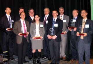
Nine research and development project teams were honored at “Transformations in Lighting,” the seventh annual U.S. Department of Energy (DOE) Solid-State Lighting (SSL) R&D Workshop, held this year in Raleigh, North Carolina. The three-day event brought together more than 350 researchers, manufacturers, and other industry insiders and observers interested in keeping up to date on the latest solid-state lighting technology developments.
At that meeting, nine significant breakthroughs and achievements in 2009 were recognized. Among them, EFRC scientist Andy Armstrong was recognized for his ongoing development of deep level optical spectroscopy (DLOS), a technique for depth-resolved characterization of point defects in wide bandgap semiconductors. The technique is of special interest in the study of the high-In-content InGaN materials that emit in the deep green, but suffer from much lower electrical-to-optical power conversion efficiency. The technique will also play a central role in EFRC studies of the fundamental mechanisms by which defects mediate radiative and non-radiative capture of electrons and holes, particularly in wide bandgap semiconductors for which the lattice distortions associated with such capture can be large and highly anharmonic.
Jeff Tsao and Mary Crawford Invited Talks at Photonics West
January 23, 2010

EFRC scientists Jeff Tsao and Mary Crawford gave invited talks at this week’s SPIE Photonics West in Moscone Center, San Francisco.
Jeff’s talk was on “Solid-State Lighting: Science, Technology and Economic Perspectives,” and was the second (after Shuji Nakamura of UCSB) of two plenary talks in the opening session for the OPTO Symposium. Jeff’s talk reviewed past, present and possible-future trajectories of solid-state lighting from a broad range of science, technology and economics perspectives. In the past: the efficiency with which power is converted into usable light has increased 2.8 orders of magnitude over three centuries, fueling large increases in the consumption of light and productivity of human society. In the present: a new technology, solid-state lighting, has emerged which promises higher efficiencies still. In the future: there is no fundamental reason why ultra (>70%) efficient solid-state lighting cannot be achieved, but significant challenges must be overcome. Among them: the elimination of blue LED droop; the development of narrow-linewidth shallow-red color converters; and the “filling in” of the red-yellow-green electroluminescence gap. (A video of Jeff’s full presentation is available for viewing.)
Mary’s talk was on “Understanding Efficiency Limitations of InGaN Quantum Wells,” in a session on Internal Quantum Efficiency and Efficiency Droop. Mary’s talk reviewed ongoing efforts aimed at understanding the low power-conversion efficiencies observed in the higher-In-content InGaN alloys which emit light in the so-called green “valley-of-death.” A principal conclusion is that point-defect-mediated non-radiative recombination appears to play an important role in the low power-conversion efficiencies. As In content increases: epitaxial growth temperatures must decrease; point defect densities increase; the concentration of deep levels associated with these point defects also increase; and photoluminescence efficiency decreases. The co-authors on Mary’s talk were Dan Koleske, Steve Lee, Andy Armstrong, Nancy Missert, Karl Westlake, Mary Miller and Karen Cross.
 ECIS Highlights






 RSS
RSS Google+
 Twitter
 Facebook
 LinkedIn
 YouTube
 Flickr

