About the Center for Nanoscale Science and TechnologyPurposeThe NIST Center for Nanoscale Science and Technology (CNST) supports the U.S. nanotechnology enterprise from discovery to production by providing industry, academia, NIST, and other government agencies with access to world-class nanoscale measurement and fabrication methods and technology. The CNST is the only national nanocenter with a focus on commerce. The CNST's shared-use NanoFab gives researchers economical access to and training on a state-of-the-art tool set required for cutting-edge nanotechnology development. The simple application process is designed to get projects started in a few weeks. Looking beyond the current state of the art, CNST research is creating the next generation of nanoscale measurement instruments and methods, which are made available through collaboration. As the Department of Commerce nanocenter, the CNST provides:
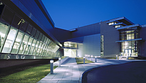
Mission and ImpactThe CNST was established in May of 2007 as a unique national facility to accelerate innovation in nanotechnology-based commerce. Its mission is to safely and reliably operate a national, shared resource for nanoscale fabrication and measurement and develop innovative nanoscale measurement and fabrication capabilities to support researchers from industry, academia, NIST, and other government agencies in nanoscale technology from discovery to production. The Center, located in NIST’s Advanced Measurement Laboratory Complex on the Gaithersburg, MD campus, disseminates new nanoscale measurement methods by incorporating them into facility operations, collaborating and partnering with others, and providing international leadership in nanotechnology. The NanoFabThe NanoFab provides researchers rapid access to a comprehensive suite of tools and processes for nanofabrication. This world-class shared resource provides researchers with a unique combination of a simple application process, extensive tool and process development, hands-on training, and access to NIST-wide expertise in nanoscience and nanotechnology. The NanoFab features a large, dedicated cleanroom, with all the tools operated within an 8,000 square foot (750 m2) class 100 space, or in adjacent laboratories that have superior air quality along with vibration, temperature, and humidity control. Over 65 major tools are available for electron beam lithography, photolithography, nano–imprint lithography, laser writing and mask generation, field emission scanning electron microscopy, metal deposition, plasma etching, chemical vapor deposition, atomic layer deposition, and silicon micro/nano-machining. The NanoFab is accessible through a straightforward application process designed to get projects started in a few weeks. It is open from 7 am to 7 pm, Monday through Friday. (Operating hours will be expanded to midnight in July of 2010.) See the NanoFab web page and contact the NanoFab Manager for detailed guidance on NanoFab access policies, procedures, and costs. A comprehensive list of the NanoFab equipment can be found on the NanoFab web page. Of particular note are the electron beam lithography tools, which include a Vistec VB300 in the cleanroom with <10 nm line width, and a JEOL JBX-6300FS, system with comparable capabilities outside the cleanroom. The lithography suite also includes a Heidelberg laser pattern generator and a Nanonex nano-imprint system. Other important capabilities are enabled by a Zeiss NVision 40 focused ion beam (FIB) system incorporating a Gemini scanning electron microscope and four-channel gas injection system. It can accommodate from mm-sized samples to 100 mm-diameter wafers for nanometer scale patterning, etching, nanomanipulation, and TEM sample preparation. CNST ResearchThe Center’s research is agile and highly interactive by design, with significant contributions from a rotating cadre of postdoctoral researchers and many collaborative projects both with NIST scientists and with others from across the US and abroad. The research staff members are organized into three Groups:
The CNST is currently giving priority to the following three research areas:
The Center's Project Leaders address these priority areas collaboratively by applying a broad range of expertise, including:
|
Contact
Center for Nanoscale Science (301) 975-8001 Telephone Gaithersburg, MD 20899-6200
|

