CNST Nanotechnology Seminar Series - 2007
| FRIDAY |
DECEMBER 7, 2007, 2:00 PM - Bldg 215, Rm C103-106 |
|
 COUPLING NANOMECHANICAL MOTION TO ELECTROMAGNETIC FIELDS THROUGH THE CASIMIR EFFECT AND SURFACE EVANESCENT WAVES COUPLING NANOMECHANICAL MOTION TO ELECTROMAGNETIC FIELDS THROUGH THE CASIMIR EFFECT AND SURFACE EVANESCENT WAVES
Ho Bun Chan
Department of Physics, University of Florida
The miniaturization of mechanical devices opens new opportunities for investigating and exploiting novel phenomena that occur for components in close proximity. The Casimir force, for example, originates from the zero-point quantum fluctuations of the electromagnetic fields. I will describe experiments that demonstrated the Casimir effect in micromechanical devices.
In another effort, subwavelength structures are fabricated on the surface of metal films to strongly modify their interaction with light. The evanescent fields channel the optical energy to specific locations, resulting in strong and localized field enhancement. Coupling of the enhanced evanescent field to the nanomechanical motion of the metallic elements opens new opportunities for tunable optical elements and high sensitivity displacement detection.
|
| |
| MONDAY |
NOVEMBER 26, 2007, 10:30 AM - Bldg 215, Rm C103-106 |
|
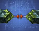 VIBRONIC EFFECTS IN SUPERCONDUCTING NANOWIRES AND MOLECULAR CONTACTS VIBRONIC EFFECTS IN SUPERCONDUCTING NANOWIRES AND MOLECULAR CONTACTS
Alexei Marchenkov
School of Physics, Georgia Institute of Technology
The generation of high-frequency current oscillations when a constant voltage is applied across an insulating tunnel gap separating two superconductors was one of the celebrated predictions made by B. Josephson in 1962. I will present evidence that Josephson current oscillations interact with atomic-scale mechanical motion. We generated weak links that contain a single niobium dimer (Nb2) suspended between two bulk niobium electrodes. We found spectral features in the electronic transport curves through the dimer, which correspond to excitations of its vibrational eigenmodes by Josephson current oscillations. This phenomenon persists up to the frequency of about 10 terahertz. This is applications-rich but largely unexplored frequency range ("terahertz gap"), which interrogates the lowest frequency vibrational modes of complex organic and biological molecules. I will describe possible applications in the fields of chemical and biological material sensing and characterization.
|
| |
| FRIDAY |
OCTOBER 26, 2007, 1:30 PM - Bldg 215, Rm C103-106 |
|
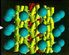 BIOLOGICAL MACROMOLECULES AS SCAFFOLDING FOR PRECISELY ENGINEERED NANOSTRUCTURES BIOLOGICAL MACROMOLECULES AS SCAFFOLDING FOR PRECISELY ENGINEERED NANOSTRUCTURES
Lee Makowski
Biosciences Division, Argonne National Laboratory
We are currently developing a system for using biological macromolecules as scaffolding for the construction of nanostructures comprising multiple inorganic nanoparticles. The system utilizes the geometry of the macromolecules to define the three-dimensional arrangement of inorganic particles in the structure. A massively parallel assembly process will be used to provide for the mass production of identical nanostructures. We envision applications to include, for example, (i) construction of small assemblies of metallic nanoparticles to form nanolenses capable of focusing surface plasmons and (ii) the construction of magnetic cellular automata.
|
| |
| THURSDAY |
JULY 26, 2007, 10:30 AM - Bldg 215, Rm C103-106 |
|
 ON CONTROL OF MICRO-SCALE SYSTEMS: COMBINING MODELING, CONTROL, SENSING, AND ACTUATION TO ACHIEVE NEW CAPABILITIES ON CONTROL OF MICRO-SCALE SYSTEMS: COMBINING MODELING, CONTROL, SENSING, AND ACTUATION TO ACHIEVE NEW CAPABILITIES
Benjamin Shapiro
Aerospace Engineering Department, University of Maryland
Modeling, design, and control of micro-scale devices for bio-chemical and medical applications. The focus is on applications where control can dramatically improve or allow new system capabilities. We consider all aspects of the design pathway from initial application choice, to system modeling, device fabrication, phrasing of design tasks as tractable mathematical problems, control algorithm development, and experimental demonstration and validation. Projects include steering of cells by micro flow control, precision control of electrowetting flows, modeling and control of bio-compatible conducting plastic micro-actuators, monitoring cells on chip, and magnetically targeted deep-tissue drug delivery.
|
| |
| THURSDAY |
MAY 17, 2007, 10:30 AM - Bldg 215, Rm C103-106 |
|
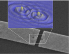 SPIN TRANSFER INDUCED SWITCHING AND DYNAMICS IN MAGNETIC NANOSTRUCTURES SPIN TRANSFER INDUCED SWITCHING AND DYNAMICS IN MAGNETIC NANOSTRUCTURES
William Rippard
Electromagnetics Division, NIST
In typical magnetic devices and measurements, the magnetization states of the elements are controlled with applied magnetic fields. However, over the last several years it has been shown that the magnetization state of ferromagnetic devices can be similarly controlled by a dc spin-polarized current passing through the device, via the so-called "spin-transfer interaction". This represents a fundamentally new way to manipulate ferromagnetic materials and is particularly important at device dimensions below about 100 nm. In this talk I will give an introduction to the spin transfer effect, and a general overview of our work using the spin transfer interaction to induce high-speed (< 500 ps) switching and coherent high-frequency (> 40 GHz) large-amplitude precession in magnetic nanostructures.
|
| |
| THURSDAY |
APRIL 19, 2007, 10:30 AM - Bldg 215, Rm C103-106 |
|
 MAGNETISM ON THE NANOSCALE MAGNETISM ON THE NANOSCALE
Andreas J. Heinrich
IBM Almaden Research Center
Understanding and controlling the magnetic properties of nanoscale systems is crucial for the implementation of future data storage and computation paradigms. Here we show how the magnetic properties of individual atoms can be probed with a low-temperature, high-field scanning tunneling microscope when the atom is placed on a thin insulator. In extended one-dimensional spin chains, which we build one atom at a time, we find strong spin-coupling into collective quantum-spins, even for the longest chains of length 3.5nm. The spectroscopic results can be understood with the model of spin-excitations in a system with antiferromagnetic coupling, controlled on the atomic scale.
|
| |
| MONDAY |
APRIL 23, 2007, 10:30 AM - Bldg 215, Rm C103-106 |
Special joint seminar with the NIST Surface and Microanalysis Science Division
 THE SECRET LIFE OF NANOPARTICLES: CHARACTERISTICS OF NANOPARTICLES AND NANOSTRUCTURED MATERIALS THAT ARE FREQUENTLY FORGOTTEN OR IGNORED THE SECRET LIFE OF NANOPARTICLES: CHARACTERISTICS OF NANOPARTICLES AND NANOSTRUCTURED MATERIALS THAT ARE FREQUENTLY FORGOTTEN OR IGNORED
Donald R. Baer
Pacific Northwest National Laboratory
Although it is generally accepted that nanoparticles and nano-structured materials are mostly surfaces or interfaces, the impacts of the nature of that surface are often ignored or minimized. Surface and interface contamination is present on many nanoparticles and may be, in the words of one colleague "the dirty secret" of nanotechnology. It has been demonstrated that the nature of the environment around nanoparticles can alter the structure of the particles. The properties of individual nanoparticles or isolated nanoparticles can also be altered when they are assembled or packed into aggregate systems, even if there is no significant binding or chemical interactions. The effective media of the aggregate will have properties that differ from the individual particles. Some of these effects will be described based on our studies of iron oxide and ceria oxide nanoparticles and other work in the literature.
|
| |
| THURSDAY |
APRIL 12, 2007, 10:30 AM - Bldg 215, Rm C103-106 |
|
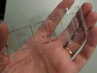 TRANSPARENT OXIDE SEMICONDUCTORS FOR FLEXIBLE AND NANO-ELECTRONICS TRANSPARENT OXIDE SEMICONDUCTORS FOR FLEXIBLE AND NANO-ELECTRONICS
Gregory S. Herman
Hewlett-Packard Company
Transparent oxide semiconductors have been extensively studied due to the direct commercial applications including displays, solar cells, sensors, and energy-efficient windows. There has been an increased interest in transparent electronics due to the possibility of forming active transparent components, which can enable new optoelectronic applications. The synthesis, characterization, and integration of these materials will be presented. We are focusing on several ternary oxides, including Zn2In2O5 and ZnSnO3. These materials have been determined to be amorphous as deposited and have excellent electrical properties when used as channel materials for thin film transistors on flexible substrates. Initial results will also be presented for ternary oxide nano-materials.
|
| |
| THURSDAY |
MARCH 22, 2007, 10:30 AM - Bldg 215, Rm C103-106 |
|
 HIGH-RESOLUTION ATOMIC FORCE MICROSCOPY: WHERE ARE WE, AND WHERE WILL THE FUTURE TAKE US? HIGH-RESOLUTION ATOMIC FORCE MICROSCOPY: WHERE ARE WE, AND WHERE WILL THE FUTURE TAKE US?
Udo D. Schwarz
Department of Mechanical Engineering, Yale University
In this talk, I will discuss the obstacles that have to be overcome to achieve high-resolution images using AFM. As we will see, the techniques that we have to apply vary depending on the specific kind of samples we are interested in. While soft biological samples require liquid environment and extremely low tip-sample interaction forces, other samples are best imaged in ultrahigh vacuum, possibly even at low temperatures. Whatever the sample, however, AFM is in principle able to deliver high-resolution images on all material classes, no matter how delicate. An example is given in the illustration, featuring a 3D atomic-scale image of crystalline xenon, which cannot be obtained with any other technique. We will further elaborate where the limitations of current state-of-the-art high-resolution AFM imaging are, and where possibilities for progress exists.
|
| |
| MONSDAY |
MARCH 12, 2007, 10:30 AM - Bldg 215, Rm C103-106 |
Special joint seminar with the NIST Intelligent Systems Division
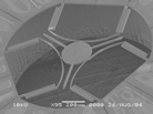 SMALL-SCALE, SIX-AXIS NANOPOSITIONERS: NEW CONCEPTS AND PERFORMANCE LIMITS FOR NANOMANUFACTURING EQUIPMENT/INSTRUMENTATION SMALL-SCALE, SIX-AXIS NANOPOSITIONERS: NEW CONCEPTS AND PERFORMANCE LIMITS FOR NANOMANUFACTURING EQUIPMENT/INSTRUMENTATION
Martin L. Culpepper
Rockwell International Associate Professor, Massachusetts Institute of Technology
The purpose of my work is to generate new concepts and the corresponding knowledge that enables the design/fabrication/implementation of small-scale, six-axis nanopositioning systems. In this talk, we will discuss the utility of smaller-scale nanopositioners and their performance limits. We will examine several new machine elements (silicon-based elements and nascent designs for carbon nanotube-based elements) and the nanopositioners that have been created using these elements. We will also discuss the high-level aspects of case studies where these devices are being created for probe-based nanofabrication processes. The case studies are the result of collaborations wherein we have partnered with process researchers in order to co-develop process-equipment pairs for future nanofabrication processes.
|
| |
| THURSDAY |
MARCH 1, 2007, 10:30 AM - Bldg 215, Rm C103-106 |
|
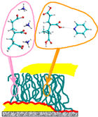 ELECTRONIC CONDUCTING STATES IN NANO- AND MESOSCALE MOLECULAR DEVICES ELECTRONIC CONDUCTING STATES IN NANO- AND MESOSCALE MOLECULAR DEVICES
Nikolai Zhitenev
Bell Labs., Alcatel-Lucent
Organic materials can offer new electronic functionality not available in the inorganic devices. However, the integration of organics within nanoscale electronic circuitry poses new challenges for material physics, chemistry and nanofabrication.
I will discuss different approaches to engineer useful electronic properties in small molecular devices. In the first case, the electronic functionality is to be provided by the backbones of short molecules. We have developed a set of fabrication and characterization techniques allowing us to build devices with self-assembled monolayers from nearly single-molecule size up to ~300 nm on a side. In the second approach, we build devices with monolayers of macromolecules. The electronic properties are determined by the composition, the chemical conversions and electric-field-induced chemical reactions of the side groups.
|
| |
| THURSDAY |
FEBRUARY 8, 2007, 10:30 AM - Bldg 215, Rm C103-106 |
|
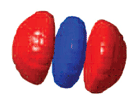 A SUMMARY OF JOINT INDUSTRY STRATEGIC RESEARCH NEEDS AND EMERGING MATERIALS WITH HIGH APPLICATION IMPACT POTENTIAL A SUMMARY OF JOINT INDUSTRY STRATEGIC RESEARCH NEEDS AND EMERGING MATERIALS WITH HIGH APPLICATION IMPACT POTENTIAL
Daniel Herr
Director, Nanomanufacturing Sciences Research, Semiconductor Research Corporation
In 2006, the Semiconductor Research Corporation’s research community, with colleagues from several other industries and government laboratories, identified a joint set of critical research needs1 in the area of nanomaterials modeling and verification. The goal was to develop an enhanced predictive capability of nanomaterials structure-property correlations and enable robust high performance application specific nanomaterials by design. Predictive models are needed for the integrated optimization of: the synthesis of nanoparticles, surface chemical reactivity, electronic and transport properties, nanomechanical properties, properties of self-assembled materials, and other application properties. Some nanomaterials families possess unique properties that make them candidates to enhance or replace conventional materials and approaches, but the need for optimization of multiple properties requires models that correlate atomic and nanostructure and local environments to desired properties. This presentation will summarize a joint set of strategic modeling and characterization needs, which are shared by multiple industries, and propose a framework for collaboratively engaging industrial, academic, and government research communities. Additionally, it will provide a summary of strategic research opportunities in several enabling material systems and emerging high potential impact application areas.
|
| |
| THURSDAY |
JANUARY 25, 2007, 10:30 AM - Bldg 215, Rm C103-106 |
|
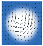 MEASUREMENT AND CHARACTERIZATION CHALLENGES FOR BEYOND CMOS NANOELECTRONICS MEASUREMENT AND CHARACTERIZATION CHALLENGES FOR BEYOND CMOS NANOELECTRONICS
George Bourianoff
Technology Manufacturing Group, Intel Corporation
Intel believes that silicon based CMOS technology will remain the workhorse of information processing technology for approximately the next 15 years and beyond that, silicon will form the platform upon which alternative information processing technologies will be built and integrated. This presentation will survey the long range research relating to the search for beyond CMOS logic alternatives. It will focus on measurement and characterization challenges associated with using alternative state variables such as magnetization, polarization and spin and the interaction of these variables with applied and induced fields. The measurement and characterization challenges are magnified by the likely introduction of new material systems and the need to ultra high spatial and temporal resolution. This presentation will draw heavily on ideas developed within the ITRS ERD and implemented in the Nanotechnology Research Initiative and Focused Center Research Programs.
(Image courtesy of Y. Acermman, Stanford University)
|
| |
| WEDNESDAY |
JANUARY 17, 2007, 10:30 AM - Bldg 215, Rm C103-106 |
|
 MAPPING UNCOMPENSATED SPINS IN EXCHANGE-BIASED SYSTEMS: RECENT DEVELOPMENTS TOWARDS AN IDEAL SCANNING FORCE MICROSCOPE MAPPING UNCOMPENSATED SPINS IN EXCHANGE-BIASED SYSTEMS: RECENT DEVELOPMENTS TOWARDS AN IDEAL SCANNING FORCE MICROSCOPE
Hans J. Hug
Empa, Dübendorf, Switzerland
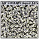
Magnetic Force Microscopy is an ideal tool to image magnetic stray fields emanating from surfaces but also from hidden interfaces of magnetic or superconducting samples. A lateral resolution of 10nm is routinely obtained on flat samples. Tip calibration techniques were developed for a quantitative evaluation of the magnetic surface charge or surface dipole density from the measured MFM signal. The latter was performed to map the spatial density of pinned uncompensated spins (UCS) in exchange-biased ferromagnet/antiferromagnet multilayers. In order to further characterize these samples, different magnetization histories in magnetometry and magnetic force microscopy measurements were used advantageously to demonstrate the co-existence of pinned UCS that are parallel and antiparallel to the cooling field in metallic (IrMn) and oxidic (CoO) EB systems. We found that the exchange-bias-effect (EB-effect) is a result of pinned interfacial UCS, which are antiparallel to the spins of the ferromagnet. The often observed positive vertical shift of the magnetization loop after field cooling is due to pinned UCS that align parallel to the cooling field, but are of little importance for the EB-effect. Whereas magnetic force microscopy seems to reach its final state of development, considerable instrumental progress remains to be achieved in scanning force microscopy with true atomic resolution. A scanning force microscope optimized for surface science would allow the simultaneous measurement of vertical and lateral forces, energy loss and tunneling current. Our recent developments will be discussed.
|
| |
| FRIDAY |
JANUARY 12, 2007, 1:30 PM - Bldg 215, Rm C103-106 |
|
 IMAGING MAGNETIC SURFACES WITH ATOMIC RESOLUTION IMAGING MAGNETIC SURFACES WITH ATOMIC RESOLUTION
Matthias Bode
University of Hamburg, Institute of Applied Physics and Microstructure Research Center
Fueled by the ever increasing data density in magnetic storage technology and the need for a better understanding of the physical properties of magnetic nanostructures, there exists a strong demand for high resolution, magnetically sensitive microscopy techniques. The technique with the highest available resolution is spin-polarized scanning tunneling microscopy (SP STM) which combines the atomic resolution capability of conventional STMs with spin sensitivity by making use of the tunneling magnetoresistance effect between a magnetic tip and a magnetic sample surface. Beyond the investigation of ferromagnetic surfaces, thin films, and epitaxial nanostructures with unforeseen precision, it also allows the achievement of a long-standing dream: the real space imaging of atomic spins in antiferromagnetic surfaces.
The lecture addresses a wide variety of phenomena in surface magnetism which in most cases could not be imaged directly before the advent of SP-STM. After starting with a brief introduction of the basics of the contrast mechanism, recent major achievements will be presented, like the direct observation of the atomic spin structure of domain walls in antiferromagnets and the visualization of thermally driven switching events in superparamagnetic particles consisting of a few hundreds atoms only. To conclude the lecture, recently observed complex spin structures containing 15 or more atoms will be presented.
|
| |
| TUESDAY |
JANUARY 9, 2007, 10:30 AM - Bldg 215, Rm C103-106 |
|
 PHAT PHOTONS FOR NIFTY NANOSCIENCE PHAT PHOTONS FOR NIFTY NANOSCIENCE
Steven R. J. Brueck
Center for High Technology Materials, University of New Mexico
Progress in optical lithography has paced the enormous progress in integrated circuits. Thus, the question of the ultimate capabilities of optical lithography is of great importance as we proceed into the deep sub-wavelength regime. The spatial frequency transmission bandwidth of free-space is 2/λ, leading to a dense (equal line/space) pattern at a half-pitch of λ/4 (or 48 nm for a 193-nm λ). Immersion provides another factor of ∼ 1.44 (H2O) or greater down to a ½ pitch CD < 33 nm. Nonlinear processes, based on photoresist chemistry and pattern transfer, allow further extension of optics beyond the single-exposure linear-systems limits, much as frequency multiplication processes allow extension of fundamental laser frequencies. The conclusion is that there is no fundamental limit to the resolution of optical lithography; there remain process latitude and manufacturing (e.g. cost) issues.
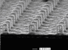
For many nanotechnology applications, large numbers of nanostructures covering a large sample area with a well-defined long-range order are required. One such example is a metamaterial with a structure- (as opposed to material-) dependent resonance. The figure shows an infrared metamaterial (an assemblage of LC tank circuits). Negative-index materials (NIMs) are another emerging area. Photonic crystals – periodic arrays of nanoscale structures (with or without aperiodic defects) – providing another example of the exciting physics accessible with current interferometric lithography capabilities. Nanostructuring for semiconductor materials development and nanofluidics for biological applications are other emerging research directions. The overall message is that a nanoscale lithography capability enables many exciting nanotechnology research directions.
|
| |
| THURSDAY |
JANUARY 4, 2007, 10:30 PM - Bldg 215, Rm C103-106 |
|
 NANOELECTROMECHANICAL SENSING AND METROLOGY: RECENT PROGRESS NANOELECTROMECHANICAL SENSING AND METROLOGY: RECENT PROGRESS
Kamil L. Ekinci
Aerospace and Mechanical Engineering, Boston University
Nanoelectromechanical systems (NEMS) have been at the center of recent applied and fundamental research. Most NEMS are resonant devices —much like simple tuning forks— with submicron dimensions. In this size regime, NEMS come with extremely high fundamental resonance frequencies, diminished active masses and tolerable force constants; the quality (Q) factors of resonance are in the range Q∼103-105. These attributes collectively make NEMS suitable for a multitude of technological applications— such as ultrasensitive force and mass sensing, narrow band filtering, and time keeping. From a fundamental physics point of view, NEMS are expected to enable the observation of quantum behavior in mesoscopic mechanical systems.
This presentation will start with a brief description of our recent work on nanomechanical mass sensing. It will then outline some of the challenges involved in realizing a practical NEMS mass sensor and focus on our efforts in addressing these challenges. One of the challenges, namely the operation of a nanomechanical resonator in a rarefied gas atmosphere, has led us to re-investigate a well-known fluid dynamics problem: Stokes’ second problem of an oscillating plate in a fluid. At the frequencies of NEMS motion, Stokes’ second problem needs to be reformulated in order to accurately describe NEMS motion. On the other hand, our efforts to develop tunneling displacement transducers have resulted in progress towards a functional radio-frequency scanning tunneling microscope (STM).
|
| |
|
|