| November 12, 2008

[NIST Tech Beat Search] [Credits] [NIST Tech Beat Archives] [Media Contacts] [Subscription Information]

Cold Atoms Could Replace Hot Gallium in Focused Ion Beams
 |
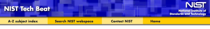
NIST researcher Jabez McClelland makes adjustments on the new magneto-optical trap ion source, capable of focusing beams of ions down to nanometer spots for use as a 'nano-scalpel' in advanced electronics processing.
Credit: Holmes, NIST
View hi-resolution image |
Scientists at the National Institute of Standards and Technology (NIST) have developed a radical new method of focusing a stream of ions into a point as small as one nanometer (one billionth of a meter).* Because of the versatility of their approach—it can be used with a wide range of ions tailored to the task at hand—it is expected to have broad application in nanotechnology both for carving smaller features on semiconductors than now are possible and for nondestructive imaging of nanoscale structures with finer resolution than currently possible with electron microscopes.
Researchers and manufacturers routinely use intense, focused beams of ions to carve nanometer-sized features into a wide variety of targets. In principle, ion beams also could produce better images of nanoscale surface features than conventional electron microscopy. But the current technology for both applications is problematic. In the most widely used method, a metal-coated needle generates a narrowly focused beam of gallium ions. The high energies needed to focus gallium for milling tasks end up burying small amounts in the sample, contaminating the material. And because gallium ions are so heavy (comparatively speaking), if used to collect images they inadvertently damage the sample, blasting away some of its surface while it is being observed. Researchers have tried using other types of ions but were unable to produce the brightness or intensity necessary for the ion beam to cut into most materials.
The NIST team took a completely different approach to generating a focused ion beam that opens up the possibility for use of non-contaminating elements. Instead of starting with a sharp metal point, they generate a small “cloud” of atoms and then combine magnetic fields with laser light to trap and cool these atoms to extremely low temperatures. Another laser is used to ionize the atoms, and the charged particles are accelerated through a small hole to create a small but energetic beam of ions. Researchers have named the groundbreaking device “MOTIS,” for “Magneto-Optical Trap Ion Source.” (For more on MOTs, see “Bon MOT: Innovative Atom Trap Catches Highly Magnetic Atoms,” NIST Tech Beat Apr. 1, 2008.)
“Because the lasers cool the atoms to a very low temperature, they’re not moving around in random directions very much. As a result, when we accelerate them the ions travel in a highly parallel beam, which is necessary for focusing them down to a very small spot,” explains Jabez McClelland of the NIST Center for Nanoscale Science and Technology. The team was able to measure the tiny spread of the beam and show that it was indeed small enough to allow the beam to be focused to a spot size less than 1 nanometer. The initial demonstration used chromium atoms, establishing that other elements besides gallium can achieve the brightness and intensity to work as a focused ion beam “nano-scalpel.” The same technique, says McClelland, can be used with a wide variety of other atoms, which could be selected for special tasks such as milling nanoscale features without introducing contaminants, or to enhance contrast for ion beam microscopy.
* J. L. Hanssen, S. B. Hill, J. Orloff and J. J. McClelland. Magneto-optical trap-based, high brightness ion source for use as a nanoscale probe. Nano Letters 8, 2844 (2008).
Media Contact: Mark Bello, mark.bello@nist.gov, (301) 975-3776 
‘Femtomolar Optical Tweezers’ May Enable Sensitive Blood Tests
 |
Basic scheme of an optical tweezer-based sensor of biological particles. A microsphere covered with a specific antigen (such as a virus or other infectious agent) is trapped and pulled away from a surface containing the corresponding antibodies. The minimum amount of force applied to the tweezers to break the bonds can provide information on the concentration of antibodies on the surface.
Credit: NIST
View hi-resolution image |
Cutting-edge “tweezers” are so sensitive that they can feel the tell-tale tug of tiny concentrations of pathogens in blood samples, yet don’t ever need to be sterilized—or even held—as they are ephemeral and weightless. The National Institute of Standards and Technology (NIST) has licensed a patented “optical tweezers” technique for detecting and measuring very small concentrations of a biological substance—such as a virus on a surface. NIST has issued a non-exclusive license for the technology to Haemonetics, a global health care company that provides blood management technologies for hospitals and blood and plasma collection agencies.
Optical tweezers are actually tightly focused laser beams. They can trap certain objects, such as latex microspheres or biological cells, and move them around in water. This occurs because the lasers' electric fields interact with electric charges on the objects.
To detect disease-causing agents, researchers can coat a microsphere with antibody particles and then touch it to a surface containing infectious particles (antigens). The antigens then stick to the antibodies on the sphere, reminiscent of Velcro, in which loops on one strip combine with hooks on the other. By determining how much laser power is required to pull the microsphere away from the surface, one can then calculate the amount of force needed to break off the antibodies from the antigens and thus count the number of individual antigens that were bound to the sphere. This in turn can detect and count biological antigens at extraordinarily low “femtomolar” concentrations—roughly equivalent to one antigen particle per quadrillion (1,000,000,000,000,000) water molecules.
Following up on earlier work in optical tweezers in the industrial and academic research communities in the 1970s, the licensed technology was patented in 1997 (patent #5,620,857), as a result of research conducted under the NIST BioSensor Consortium. The inventors are Howard Weetall (since retired), Kristian Helmerson, and guest researcher Rani Kishore.
For more information on these or other NIST technologies, should contact Terry Lynch, NIST Office of Technology Partnerships, terry.lynch@nist.gov, (301) 975-2691.
Media Contact: Ben Stein, ben.stein@nist.gov, (301) 975-3097
Nanoparticles in the Home: More and Smaller Than Previously Detected
 |
NIST researcher Cynthia Howard Reed and guest researcher Lance Wallace measure nanoparticles emitted by common household appliances. The new experiments can measure 'ultrafine particles' ranging in size from 2 to 10 nanometers.
Credit: NIST
View hi-resolution image |
Extremely small nanoscale particles are released by common kitchen appliances in abundant amounts, greatly outnumbering the previously detected, larger-size nanoparticles emitted by these appliances, according to new findings* by researchers at the National Institute of Standards and Technology (NIST). So-called “ultrafine particles” (UFP) range in size from 2 to 10 nanometers. They are emitted by motor vehicles and a variety of indoor sources and have attracted attention because of increasing evidence that they can cause respiratory and cardiovascular illnesses.
NIST researchers conducted a series of 150 experiments using gas and electric stoves and electric toaster ovens to determine their impacts on indoor levels of nano-sized particles. Previous studies have been limited to measuring particles with diameters greater than 10 nm, but new technology used in these experiments allowed researchers to measure down to 2 nm particles—approximately 10 times the size of a large atom.
This previously unexplored range of 2 to 10 nm contributed more than 90 percent of all the particles produced by the electric and gas stovetop burners/coils. The gas and electric ovens and the toaster oven produced most of their UFP in the 10 nm to 30 nm range.
The results of this test should affect future studies of human exposure to particulates and associated health effects, particularly since personal exposure to these indoor UFP sources can often exceed exposure to the outdoor UFP.
Researchers will continue to explore the production of UFP by indoor sources. Many common small appliances such as hair dryers, steam irons and electric power tools include heating elements or motors that may produce UFP. People often use these small appliances at close range for relatively long times, so exposure could be large even if the emissions are low.
The experiments were conducted in a three-bedroom test house at NIST that is equipped to measure ventilation rates, environmental conditions and contaminant concentrations.
* L. Wallace, F. Wang, C. Howard-Reed and A. Persily. Contribution of gas and electric stoves to residential ultrafine particle concentrations between 2 and 64 nm: Size distributions and emission and coagulation rates. Environmental Science and Technology, DOI 10.1021/es801402v, published online Oct. 30, 2008.
Edited on Nov. 13, 2008 to correct copy.
Media Contact: Evelyn Brown, evelyn.brown@nist.gov, (301) 975-5661
Improved Measurements Could Mean Safer, More Reliable Electroshock Weapons
Electroshock weapons—such as stun guns and other similar devices that temporarily incapacitate a person by delivering a high-voltage, low-current electric shock—have helped law enforcement officers safely subdue dangerous or violent persons for years. The use of these weapons has been challenged, however, by claims that they may have contributed to more than 150 deaths in the United States since 2001. Now, researchers at the National Institute of Standards and Technology (NIST) are working toward a standard method for accurately assessing the electrical output of these devices, the results of which can be used in establishing baselines for future medical and safety studies.
Groups such as Amnesty International have called for guidelines for electroshock weapons that include “threshold exposures” (the minimum charges that would incapacitate different groups of people without putting them at risk for injury or death). One obstacle to the development of such guidelines is the fact that various reports regarding the output of electroshock weapons—the current and voltage they deliver—are inconsistent.
To address this problem, scientists in NIST’s Office of Law Enforcement Standards (OLES) have developed methods for calibrating the high-voltage and current measurement probes used by industry so that any inherent biases in the probes are minimized. By compensating for these probe effects, voltage and current readings were obtained that reflect the energies being dispensed by the weapons.
Next steps in the characterization program for electroshock weapons include implementing a second type of high-voltage measurement to verify the probe calibration system; further refining the uncertainty analysis for the overall measurement method to better define its accuracy and reliability; and, eventually, working with government agencies and the law enforcement community to standardize the method that will facilitate establishment of use guidelines.
For more information, contact Nicholas Paulter, nicholas.paulter@nist.gov, (301) 975-2405.
Media Contact: Michael E. Newman, michael.newman@nist.gov, (301) 975-3025
Iron-based Materials May Unlock Superconductivity’s Secrets
 |
NIST researchers have found that new iron-based high-temperature superconductors subtly change their molecular shape as temperatures decrease. This graphic shows a superconductor transitioning from tetragonal (at top) to orthorhombic at about 220 Kelvin (-53 degrees Celsius). Such physical changes appear to be a precursor to superconductivity, in which electric current can flow without resistance.
Credit: NIST
View hi-resolution image |
Researchers at the National Institute of Standards and Technology (NIST) are decoding the mysterious mechanisms behind the high-temperature superconductors that industry hopes will find wide use in next-generation systems for storing, distributing and using electricity. In two new papers* on a recently discovered class of high-temperature superconductors, they report that the already complicated relationship between magnetism and superconductivity may be more involved than previously thought, or that a whole new mechanism may drive some types of superconductors.
At temperatures approaching absolute zero, many materials become superconductors, capable of carrying vast amounts of electrical current with no resistance. In such low-temperature superconductors, magnetism is a villain whose appearance shatters the fragile superconductive state. But in 1986, scientists discovered “high temperature” (HTc) superconductors capable of operating much warmer than the previous limit of 30 degrees above absolute zero. In fact, today’s copper-oxide materials are superconductive in liquid nitrogen, a bargain-priced coolant that goes up to a balmy 77 degrees above absolute zero. Such materials have enabled applications as diverse as high-speed maglev trains, magnetic-resonance imagers and highly sensitive astronomical detectors. Still, no one really understands how HTc superconductivity works, although scientists have long suspected that in this case, magnetism boosts rather than suppresses the effect.
The beginnings of what could be a breakthrough came in early 2008 when Japanese researchers announced discovery of a new class of iron-based HTc superconductors. In addition to being easier to shape into wires and otherwise commercialize than today’s copper-oxides, such materials provide scientists fresh new subjects with which to develop and test theories about HTc superconductivity’s origins.
Scientists at NIST’s Center for Neutron Research and a team including researchers from the University of Tennessee at Knoxville, Oak Ridge National Laboratory, the University of Maryland, Ames Laboratory and Iowa State University used beams of neutrons to peek into a superconductor’s atomic structure. They first found iron-based superconductors to be similar to copper-oxide materials in how “doping” (adding specific elements to insulators in or around a HTc superconductor) influences their magnetic properties and superconductivity.
Then the team tested the iron-based material** without doping it. Under moderate pressure, the volume of the material’s crystal structure compressed an unusually high 5 percent. Intriguingly, it also became superconductive without a hint of magnetism.
The iron-based material’s behavior under pressure may suggest the remarkable possibility of an entirely different mechanism behind superconductivity than with copper oxide materials, NIST Fellow Jeffrey Lynn said. Or it could be that magnetism is simply an ancillary part of HTc superconductivity in general, he said—and that a similar, deeper mechanism underlies the superconductivity in both. Understanding the origin of the superconductivity will help engineers tailor materials to specific applications, guide materials scientists in the search for new materials with improved properties and, scientists hope, usher in higher-temperature superconductors.
* J. Zhao, Q. Huang, C. de al Cruz, S. Li, J. W. Lynn, Y. Chen, M. A. Green, G. F. Chen, G. Li, Z. C. Li, J. L. Luo, N. L. Wang and P. Dai. Structural and magnetic phase diagram of CeFeAsO1-xFx and its relationship to high-temperature superconductivity. Nature Materials (DOI 10.1038/nmat2315).
A. Kreyssig, M. A. Green, Y. B. Lee, G. D. Samolyuk, P. Zajdel, J. W. Lynn, S. L. Bud’ko, M. S. Torikachvili, N. Ni, S. Nandi, J. Leão, S. J. Poulton, D. N. Argyriou, B. N. Harmon, P. C. Canfield, R. J. McQueeney and A. I. Goldman. Pressure-induced volume-collapsed tetragonal phase of CaFe2As2 as seen via neutron scattering. Phys. Rev. B 78 (in press).
** CaFe2As2
Edited Nov. 17, 2008, to correct caption.
Media Contact: Evelyn Brown, evelyn.brown@nist.gov, (301) 975-5661
Let the Games Begin! Nanosoccer at 2009 RoboCup in Austria
 |
The 2009 RoboCup Nanosoccer competition will be played on the gold-colored microchip seen through the window of the “world's smallest soccer stadium.” The chip is divided into 16 playing fields each the size of a grain of rice.
Credit: Talbott, NIST
View hi-resolution image |
The World Cup may be two years away, but soccer aficionados can get an early start at satisfying their yen for global competition when the National Institute of Standards and Technology (NIST) and the RoboCup Federation host the second-ever international nanosoccer contest next summer.
Nanosoccer—the Lilliputian competition where computer-driven “nanobots” the size of dust mites challenge one another on fields no bigger than a grain of rice—will be part of the RoboCup games in Graz, Austria, from June 29-July 5, 2009. NIST is now accepting applications for organizations wishing to field robots in the events.
Viewed under a microscope, the soccer nanobots are operated by remote control and move in response to changing magnetic fields or electrical signals transmitted across the microchip arena. “Nanoscale” refers to their mass. The bots are a few tens of micrometers to a few hundred micrometers long, but their masses range from only a few nanograms to a few hundred nanograms. They are manufactured from materials such as aluminum, nickel, gold, silicon and chromium.
Rules for the “Nanogram 2009” competition and the application form (called the “Team Description Paper”) are available at www.nist.gov/public_affairs/calmed/nanosoccer.html. The “NIST and Nanosoccer” Web site also features detailed information on nanosoccer, summaries of past competitions and a short video showing how the contests “road test” agility, maneuverability, response to computer control and the ability to move objects—all skills that future industrial nanobots will need for tasks such as microsurgery within the human body or the manufacture of tiny components for microscopic electronic devices.
NIST is jointly organizing the Nanogram 2009 events with RoboCup, an international organization dedicated to fostering innovations and advances in artificial intelligence and intelligent robotics by using the game of soccer as a testing ground. NIST’s goal in coordinating competitions between the world’s smallest robots is to show the feasibility and accessibility of technologies for fabricating MicroElectroMechanical Systems (MEMS), tiny mechanical devices built onto semiconductor chips and measured in micrometers (millionth of a meter). The contests also drive innovation in this new field of robotics by inspiring young scientists and engineers to become involved.
Teams wishing to compete in Austria must submit their application materials by Dec. 31, 2008, by either e-mail to nanogram@nist.gov or by regular mail to RoboCup Nanogram 2009, c/o Craig McGray, NIST, 100 Bureau Dr., MS 8120, Gaithersburg, Md. 20899-8120.
Media Contact: Michael E. Newman, michael.newman@nist.gov, (301) 975-3025
NIST, NCI Bring Web 2.0 Tools to Nanotechnology Standards Effort
Federal government and U.S. industry scientists say they are forging ahead with plans for an international, online collaboration to speed up creation of critically needed nanotechnology standards, including the underpinning reference materials and tests that support development of nanotech products while minimizing potential risks.
Combining efforts of materials scientists and measurement laboratories with those of biological and medical researchers, the new Internet-linked “community of interest” will exploit Web 2.0-style social networking technologies to enable creating and sharing information, as well as deliberating over technical details of in-process standards. The initial focus will be standards for characterizing the structure and properties of engineered nanoscale materials.
The global market for nanotechnology-enabled products is forecast to top $3 trillion by 2015. This anticipated stream of nanotech innovations has spawned a backlog of standards needs.
The idea for the Web-based collaboration was strongly endorsed during a recent international workshop hosted by the National Institute of Standards and Technology (NIST). A prototype wiki—or collaborative Web site—was demonstrated by representatives of the National Cancer Institute’s (NCI’s) Advanced Biomedical Computing Center.
Now undergoing further development at NCI, the nanotechnology standards wiki will enable instantaneous dissemination (as well as archival) of drafts, discussions, votes and supporting materials. Wiki-related tools will help in organizing discussions, and standards developing organizations (SDOs) will be able to tap this resource to expedite drafting and validating protocols before they enter the formal approval process.
SDOs are developing standards in the fast-moving technology area, but scientists at the workshop said the overall response is not as effective or as coherent as the global challenge requires.
NCI and its partners expect the site to be up and running by early 2009. For more information, see “NCI and NIST Propose Online Community To Speed Up Development of Nanotech Standards”.
Media Contact: Mark Bello, mark.bello@nist.gov, (301) 975-3776
Quick Links
NIST Receives 64 Submissions for New ‘Hash’ Algorithm
The National Institute of Standards and Technology (NIST) has received a total of 64 submissions for a competition to develop a new cryptographic “hash” algorithm, a tool that converts a file, message or block of data into a short “fingerprint” for use in digital signatures, message authentication and other computer security applications.
The hash algorithm ultimately chosen by NIST will be called Secure Hash Algorithm-3 (SHA-3) and will augment the hash algorithms currently specified in the Federal Information Processing Standard (FIPS) 180-3, Secure Hash Standard. FIPS standards are required for use in federal civilian computer systems and are often adopted voluntarily by private industry. (See “NIST Issues Call for a New ‘Hash’ Algorithm,” NIST Tech Beat, Nov. 8, 2007.)
The 64 submissions are currently being reviewed; they come from groups as small as one individual and as large as 15 people. Those groups whose entries are determined to be “complete and proper” according to the competition rules will be considered “first-round candidates” and they will be posted on the NIST Web site for the competition at www.nist.gov/hash-competition.
NIST, Columbia Honored for 1931 Discovery of Heavy Hydrogen
The National Institute of Standards and Technology (NIST) and Columbia University have been named by the American Chemical Society (ACS) Division of the History of Chemistry as recipients of the ACS Citation for Chemical Breakthrough Award in recognition of the isolation of deuterium, the isotope of hydrogen commonly called “heavy hydrogen.” The feat—proving that deuterium actually existed—was achieved in 1931 by physicists from the National Bureau of Standards (NBS), NIST’s predecessor, and Columbia.
The award was given to NIST during a ceremony at the agency’s headquarters in Gaithersburg, Md., on Nov. 6, 2008.
In 1931, NBS physicist Ferdinand Brickwedde collaborated with Columbia physicists Harold Urey and George Murphy to produce the first sample of deuterium at the NBS Low Temperature Laboratory in Washington, D.C. (on what is now the campus of the University of the District of Columbia). Team leader Urey was awarded the Nobel Prize in Chemistry for the discovery. Today, deuterium is used as a non-radioactive tracer in scientific and medical research and in the study of thermonuclear fusion reactions.
For more information on the first isolation of deuterium, go to http://nvl.nist.gov/pub/nistpubs/sp958-lide/043-045.pdf.
NIST Researcher Receives Kudos for Images of Labs on a Chip
National Institute of Standards and Technology (NIST) bioengineer Greg Cooksey is equally talented behind the lens of a camera as he is engineering complex microfluidic devices for biology experiments—and recently, he’s received quite a bit of recognition for combining the two skills. In the past year, Cooksey’s photomicrographs—most often portraying the colorful beauty of dyes flowing through his designs—have been showcased in the Images from the Science 2 exhibition staged by the Rochester Institute of Technology (http://www.rit.edu/cias/ritphoto/ifs-2008/photo_gallery/pages/12_cooksey_1.htm and http://www.rit.edu/cias/ritphoto/ifs-2008/photo_gallery/pages/13_cooksey_2.htm), featured in Discover Magazine (http://discovermagazine.com/photos/02-visual-tour-of-the-world-of-science) and honored as an “image of distinction” in the 2008 Nikon Small World contest (http://www.nikonsmallworld.com/gallery.php?grouping=year&year=2008&imagepos=51). Upcoming venues for Cooksey’s photographs include Science Illustrated and SEED magazines.
Two NIST Researchers’ Papers Recognized in Ceramics ‘Best Of’ Collection
Two materials scientists at the National Institute of Standards and Technology (NIST) have papers in a special list of the “11 best papers” published by the American Ceramics Society (ACerS) in the past 110 years.
The somewhat idiosyncratic list was drawn up by the society as part of its 110th anniversary celebration, and draws on papers submitted to the society’s journal from around the world since 1925. Included on the list are:
- S. M. Wiederhorn and L. H. Bolz. Stress corrosion and static fatigue of glass. J. Amer. Cer. Soc., 53 (10) 543-548 (1970), and
- G. Anstis, P. Chantikul, B. Lawn and D. B. Marshall. A critical evaluation of indentation techniques for measuring fracture-toughness: 1 - Direct crack measurements materials. J. Amer. Cer. Soc., 64 (9) 533-538 (1981).
Sheldon Wiederhorn and Brian Lawn currently are researchers in NIST’s Materials Science and Technology Laboratory. In 1981, Lawn was with the Department of Applied Physics of the University of New South Wales. For a complete list and copies of the papers, see “ACerS 11 Best Papers in 110 years” at the American Ceramics Society.
|