|

Sandia's Microelectronic Development Laboratory (MDL) was built in 1988 as a world-class facility dedicated to the advancement of microelectronic research, development, and application initiatives of strategic interest to the United States of America and the Department of Energy. There is over 180,000 square feet of laboratory space consisting of a diverse and complete tool set that supports microelectronics initiatives in failure analysis, reliability, test, modeling and simulation, advanced packaging, radiation hardness assurance, device design, and silicon device fabrication.
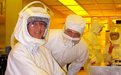
Wafer Fabrication Clean Room
  At the core of the MDL is a 30,000 square foot state-of-the-art wafer fabrication clean room. This clean room is constructed on a laminar flow modular unit design consisting of 22 separate clean room bays integrated as a single wafer processing facility providing over 12,000 square feet of Class 1 (less than 1 particle larger than 0.5 microns in size per cubic foot of air) fabrication space. Each clean room bay is supported by an independent air handling and purification system allowing for maximum flexibility in the types of projects supported within the facility. The MDL wafer fab tool set includes semiconductor wafer fabrication equipment supporting full flow CMOS integrated circuit technologies on 6" wafers. Lithography steppers of ‘G’ line, ‘I’ line, and DUV technology support minimum device feature sizes of 1.25 micron, 0.5 micron, and 0.35µm respectively. Three to four levels of metal and corresponding dielectric isolation are planarized via a state-of-the-art chemical mechanical polishing (CMP) capability.
Silicon Based Technologies
 Technologies supported by the MDL wafer fab are silicon based and focused towards Sandia National Laboratories'; mission as the steward of the nation's nuclear weapons stockpile. The center of this focus is the development and application of radiation hardened CMOS integrated circuit technologies capable of realizing digital, analog, mixed-mode, and nonvolatile memory circuits. In addition, the MDL wafer fab is the world's premier R&D source of surface micromachining technology and the integration of that technology with CMOS (IMEMS - Integrated MicroElectroMechanical Systems). Technologies supported by the MDL wafer fab are silicon based and focused towards Sandia National Laboratories'; mission as the steward of the nation's nuclear weapons stockpile. The center of this focus is the development and application of radiation hardened CMOS integrated circuit technologies capable of realizing digital, analog, mixed-mode, and nonvolatile memory circuits. In addition, the MDL wafer fab is the world's premier R&D source of surface micromachining technology and the integration of that technology with CMOS (IMEMS - Integrated MicroElectroMechanical Systems).
Capabilities
 The capabilities of the MDL wafer fab, technologies and equipment set, are leveraged to support partnerships with industry, academia, and other government agencies. Characteristic activities include benchmarking of advanced semiconductor process tools, technology development and transfer for commercial and government application, and post-doctorate research in semiconductor process and technology. The capabilities of the MDL wafer fab, technologies and equipment set, are leveraged to support partnerships with industry, academia, and other government agencies. Characteristic activities include benchmarking of advanced semiconductor process tools, technology development and transfer for commercial and government application, and post-doctorate research in semiconductor process and technology.
Professional Staff
 The
MDL's professional staff includes a core of Ph.D., Master,
and Bachelor level scientists, engineers, and technicians
who are experienced in a broad range of disciplines. The
MDL's professional staff includes a core of Ph.D., Master,
and Bachelor level scientists, engineers, and technicians
who are experienced in a broad range of disciplines.
Disciplines include:
- microelectronic and micromachining process development
- equipment design
- materials engineering
- device physics
- chemical engineering
- sensor science
- circuit design
- computer science
- failure analysis
- reliability physics
- modeling and simulation engineering
MDL Process Areas
CMP, CVD, Diffusion, Wet Process, Photolithography, Metallization, Dry Etch, Implant, and MEMS Release.
|

