|

Discovery
The World’s Smallest Fountain Pen?

New microscope tips use capillary action to print patterns tens of nanometers across
October 5, 2005
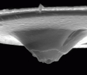
The miniscule tip on an atomic-force microscope (AFM) helps researchers both "see" and manipulate the nanoscale environment. Now, engineers have created two novel technologies that enable such tips to write features as small as viruses and to withstand abuse with the resilience of diamond. Eventually, they believe, vast arrays of such nanofountain probes could prove useful for crafting such intricate systems as protein arrays or complex semiconductors.
By taking advantage of the same capillary forces that keep fountain pens flowing, researchers from Northwestern University in Evanston, Ill., created a specialized structure that channels inks from a tiny reservoir down to a miniscule AFM tip.
Existing "dip-pen" techniques utilize the same inks, which range from pigments for creating patterns to organic materials for creating sensors, but they suffer from difficulties with maintaining a regular ink supply. The new "nanofountain probe" can paint features as small as 40 nanometers and carries its own ink reservoir.
Horacio Espinosa and colleagues from the NSF Nanoscale Science and Engineering Center for Integrated Nanopatterning and Detection Technologies crafted the probe using standard microfabrication techniques, so device production is scalable.
The center, a collaboration among researchers from Northwestern University, the University of Chicago, the University of Illinois at Urbana-Champaign and Argonne National Laboratory, was also behind the development of another AFM breakthrough: single-piece, ultra-nano-crystalline diamond cantilevers and tips.
Existing commercially available tips incorporate a diamond tip glued to a cantilever, a difficult component to craft, or less durable silicon tips coated with layers of diamond.
In addition to being extremely durable, the new tips are also crafted using standard microfabrication techniques and offer the same manufacturing advantages as the nanofountain probes.
Both developments appeared in the journal Small. A report on the nanofountain probe appeared in the April 2005 issue, and one on the ultra-nano-crystalline diamond tip appeared in the August 2005 issue.
The research was supported by NSF Grants 0304472 and 0118025
-- Josh Chamot
Investigators
Zhen Chen
Chad Mirkin
Mark Hersam
Ted Belytschko
Horacio Espinosa
Orlando Auciello
Related Institutions/Organizations
Northwestern University
Argonne National Laboratory
University of Missouri-Columbia
NSF Nanoscale Science and Engineering Center for Integrated Nanopatterning and Detection Technologies
Locations
Illinois
Missouri
Related Awards
#0118025 Nanoscale Science & Engineering Center for Integrated Nanopatterning and Detection Technologies
#0304472 NIRT: Science and Technology of Ultrananocrystalline Diamond Films for Multifunctional MEMS/NEMS Devices
Total Grants
$1,300,001
Related Agencies
Department of Energy
|