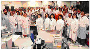
| Having experienced years
of continuous growth, CSRL capabilities are now among
the most extensive of any laboratory of its kind in
the world. We now draw upon approximately 120 personnel
from various organizations within Sandia National Laboratories;
about one third of whom are Ph.D. scientists and engineers.
 The
CSRL represents the culmination of a long-term thrust
into compound semiconductor science and technology that
began at Sandia National Laboratories in the late 1970's.
At that time, it was realized that devices based on
compound semiconductors would be necessary for photonic
applications and for microelectronic applications requiring
greater radiation hardness as well as higher speed and
operating temperatures than were available from devices
based on silicon. The
CSRL represents the culmination of a long-term thrust
into compound semiconductor science and technology that
began at Sandia National Laboratories in the late 1970's.
At that time, it was realized that devices based on
compound semiconductors would be necessary for photonic
applications and for microelectronic applications requiring
greater radiation hardness as well as higher speed and
operating temperatures than were available from devices
based on silicon.
It
was also realized that a successful effort would require
the development and integration of capabilities in solid-state
physics and chemistry, materials and process science
and technology, as well as device design and testing.
|
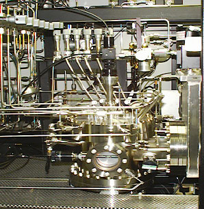
Organometallic Vapor Phase Epitaxy (OMVPE) Reactor
Supports
The CSRL fills an intermediate niche in the research
to development to applications technology cycle. It
is heavily weighted towards development, but with strong
and crucial overlaps in research and in applications
with the nation's defense-mission and commercial needs
such as:
- Microsystem Skunkworks
- Compound Semiconductor Materials Growth and Processing
- RF & Photonic Device Technologies
- Microsensors Fabrication
- Hybrid
Integration/Advanced Packaging
Advanced Processing
|
|
Accomplishments
Our capabilities and the efforts that sustain them have
grown steadily from the purchase of our first molecular
beam epitaxy (MBE) system in 1981 to the:
- Discovery of the unique electrical and optical properties
of strained-layer superlattices in 1982
- Demonstration of strain-induced light holes in 1986
- First epitaxially grown monolithic vertical-cavity
surface emitting laser (VCSEL) in 1986
- Timeframe, 1986-2000
- First large-scale monolithic integration of VCSELs
and photodiodes in 64X64 matrix addressable circuits
in 2001
- Planar lightwave circuits (PLCs) in SiON/SiO2/Si
in 2002
The CSRL serves a wide range of customers and partners,
with major DOE and DoD programs in Sandia's national
security and science mission areas, and with numerous
formal and informal collaborations.
It's projects are distinguished from those of industry
and universities by time. U.S. industry tends to focus
on work that is near term (1-3 years from product realization),
while U.S. universities tends to focus on work that
is long term (7-10 years from product realization).
In contrast, Sandia tends to focus on work that is medium
term (3-7 years from product realization).
|
|
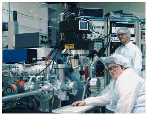
6500 Square Feet Class 100 Clean Room Space
In 1989 the CSRL completed 3700 square feet of
class 100 clean room space which was expanded to
6500 square feet in 1992.
- Nine epitaxial growth systems
- Specialized processing including
- E-beam lithography
- Ion beam etching (RIBE and CAIBE)
- High density plasma (ECR and ICP) reactive ion etching
Indeed,
the CSRL's unique ability to bridge the gap between
research and mission-driven applications is a source
of tremendous vitality and synergy. Research is
strengthened through the validation enabled by applications;
applications are strengthened through the improved
performance enabled by research.
|