to advance
measurement science at the atomic and nanometer scale,
focusing on precision optical metrology, quantum devices,
nanoscale plasmas, and nanooptical systems.
INTENDED OUTCOME AND BACKGROUND
This strategic element focuses on developing
and exploiting precision metrology
at the interface between atomic and
nanoscale systems. Systems under study
include quantum dots and wires, ultracold
atomic quantum gases, metallic
nanoparticles, and those with nanoscale
features induced on surfaces by highly
charged ions. Such systems arise in
advanced 193 nm and 157 nm lithography,
plasma etching of semiconductor
wafers, nanolasers, detectors, biomarkers
and sensors, nanomaterials, quantum
devices and quantum information, and atomic clocks.
Our research combines theory and
experiment. Theory is used to extend
the fundamental understanding of systems
at the atomic/nanoscale interface
as necessary to interpret experiment, to
explore new applications in nanoscale
and quantum technologies, and to
motivate new and enhanced precision
metrology. We are developing the
theoretical understanding needed to
create nanooptics structures that will be
needed in emerging quantum and nanoscale technologies.
Experiment is used to develop new precision
measurement tools for this
regime, to collect precise data essential
for the applications mentioned, and to
further the understanding of these systems.
We have developed precision
metrology to make accurate displacement
measurements to subatomic
dimensions by use of frequency combs
locked to a cesium atomic clock. We
have made the precise measurements of
the refractive index of water needed by
the semiconductor industry to develop
immersion lithography for sub-100 nm
optical lithography. And we are now
expanding our expertise by beginning to
probe the nanooptics and nanomechanical
properties of nanoscale and quantum-coherent systems.
Accomplishments
Designing the Nanoworld:
Nanostructures, Nanodevices,
and Nanooptics
| |
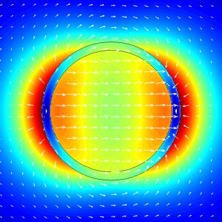
Figure 4. Field within and around a 60 nm
radius gold nanoring. Enhanced fields inside
the nanoring would make the nanoring a useful
container for precision nanoexperiments.
|
Developing and exploiting precision
metrology for quantum and nanotechnology
requires nanoscale modeling of
ultrasmall structures, devices, their
dynamical operation, and their response
to probes.
Atomic-scale simulations of the electronic
and optical properties of complex
nanosystems at the nano/molecular
interface are being carried out. These
systems include nanocrystals, self-assembled
dots, nanodot arrays and solids,
molecular electronics, and bio/nanohybrids.
These simulations provide
benchmarks for precise experimental
tests of the atomic-scale sensitivity of
nanosystems. The work is providing the
foundation needed to build design tools
for engineering nanolasers, detectors,
biomarkers and sensors, quantum
devices, and nanomaterials.
Nanoscale simulations of optical fields
near nanosystems are also being carried
out. Results are being used to design
nanoprobes and nanocavities, as shown
in Fig. 4, for use in precision nanooptics
metrology. Results are being used to
design and model the nanooptics highway,
that is, a collection of nanoparticles
used to generate, transport, and collect
photons on the nanoscale, well below
the diffraction limit that governs the
classical transport of photons.
Nanooptics highways will be critical
for the transport of excitations in
quantum devices and in the metrology
of these devices.
Subatomic Displacement
Measurements
| |
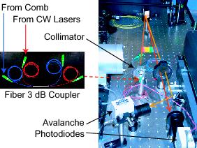
Figure 5. Setup to measure frequency difference
of 16 THz between lasers at 612 nm
and 633 nm. Light from the CW lasers is beat
against light from a visible frequency comb
in a fiber 3 dB coupler. After collimation, the
red and orange components are separated
with a grating, and the beats of the CW lasers
with adjacent comb lines are measured on
avalanche photodiodes.
|
We are concluding our program to
improve the accuracy of Michelson and
Fabry-Perot interferometry for measuring
displacements of macroscopic
objects with subatomic precision. Our
work in Fabry-Perot interferometry is
the realization of the idea first put forth
by Zoltan Bay at NBS in 1970, of using
a microwave measurement of the mode
spacing within a Fabry-Perot cavity to
measure displacements free of the systematic
error induced by diffraction.
In our most recent implementation of
Bay's idea, as shown in Fig. 5, we probe
two adjacent modes of a variable-length
Fabry-Perot cavity with red light from a
HeNe laser at 633 nm, and another
mode with orange light from a HeNe
laser at 612 nm. A precise measurement
of the mode spacing using the light at
633 nm allows us to determine the exact
number of modes in the 16 THz interval
between the red and orange lasers.
We then beat light from the HeNe lasers
against light from a visible frequency
comb that is locked to a cesium atomic
clock. The resulting measurements of
the cavity length are not compromised
by diffraction. They are related directly
to the definition of the second, and by
extension, the meter.
We are now turning our focus to the
metrology needs of microscopic systems
themselves, in particular, microelectro-mechanical
(MEMS), nanoelectro-mechanical
(NEMS), and nanooptical
systems. Precision optical and quantum
optical metrology will be exploited to
probe individual nanoscale and,
possibly, quantum-coherent systems.
Optical Properties in Support
of UV Lithography
In late 2002, the semiconductor lithography industry began an effort to
explore the feasibility of developing immersion lithography as a method to
extend optical lithography into the sub-100 nm feature-size region.
In this technology, an immersion fluid is inserted
between the final lens of a 193 nm or
157 nm lithography projection system
and the silicon wafer, thus dividing the
diffraction-limited feature size by the
refractive index of the fluid. However,
at that time there existed no accurate
measurements of the key optical properties
of water, the principal candidate
193 nm immersion fluid.
To address this need, the Atomic Physics
Division and the Optical Technology
Division teamed up to develop a UV
fluid refractive index measurement facility.
By March of 2003, the project delivered
the first accurate measurements of
the refractive index of distilled water at
193 nm to five decimal places, sufficient
for system design. The project also
delivered other key optical properties of
water, including the dependence of the
index on wavelength, temperature, pressure,
and gas and impurity content.
Immersion lithography systems using
water at 193 nm are being designed and
built around the world, relying on these
measurements as key design parameters.
The project has also characterized the
optical properties of other fluids with
significantly higher 193 nm indices than
that of water, which may potentially
enable further resolution increases. The
semiconductor industry now has a parallel
effort to explore immersion lithography
at 157 nm. The project has also
delivered the first measurements of the
key optical properties of the candidate
immersion fluids in this vacuum ultraviolet region.
Nanometrology of Highly-Charged-Ion
Collisions with Neutral Matter
| |
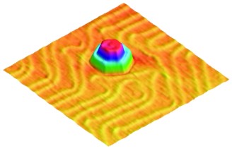
Figure 6. Scanning tunneling microscope image
(32 nm × 32 nm) of a 9 nm mound, two
atomic layers high, created by the impact of a
single Xe44+ ion on the Au(111) surface. The
mound has relaxed to a perfect hexagon, and
the "herring-bone" reconstruction in the background
has rearranged around the mound to minimize surface energy. |
Highly charged ions (HCIs) constitute a
unique and exotic form of matter, typically
out of human reach, but they can
be created and studied within the NIST
Electron Beam Ion Trap (EBIT) facility.
When neutral matter is exposed to
HCIs, the intense electronic interaction
produces extreme conditions that allow
us to probe properties of both participants,
including processes of x-ray emission,
charge exchange, and surface damage
(see Fig. 6). By coupling HCIs with
surface science techniques like scanning
tunneling microscopy, we are able to
observe electronic and morphological
changes at atomic length scales and to
probe the fundamental connections of
atomic and solid state physics.
This unique combination of capabilities
has been used to diagnose HCI damage
to advanced Mo/Si multilayer mirrors,
used for extreme ultraviolet (EUV)
lithography. Tunneling spectroscopy and
EUV reflectivity measurements have
revealed that the EUV-source ions cause
approximately ten times more damage
if they neutralize on the oxidized ruthenium
capping layer of the optics than
if they neutralize prior to collision.
These measurements highlight the broader need for providing
critical components with protection from HCIs
when operating in close proximity to
plasmas. Experiments currently underway
on gold surfaces are designed to
determine whether high-electron-density
materials exhibit less damage than insulating
and oxidized materials, currently used for critical components.

First strategic focus |
Second strategic focus |
Third strategic focus
"Technical Activities 2004" - Table of Contents |