
 At A Glance, Fall 1995
Technology at a Glance is a quarterly newsletter from the National Institute of Standards and Technology reporting on research results, funding programs, and manufacturing extension and technology services. If you have comments or general questions about this newsletter or if you would like to receive the four-page, color newsletter in hardcopy, please email your request to gail.porter@.nist.gov or call Gail Porter at (301) 975-3392. About Technology at a Glance.
In this Issue . . .
New Bioreactor Grows Blood Cells
Microscope Opens View of the Nanoworld
Making Tall Spaces More Fire Safe
Atom Lithography May Shrink "Chips"
Better Metalmaking Through Modeling
New Catalog Lists Reference Data
Shorts
- ATP Helps Zap Bugs Au Naturel
- Aging Silk with Radiation
- An Environmentally Friendly Clean
- Carbon Dating Comes of Age
Co-op Corner :
Dental Products, Auto Emissions, Data Storage, Crack Detection
New Bioreactor Grows Blood Cells
A bioreactor that provides the right environment for bone marrow cells to produce human blood cells has been developed by Aastrom Biosciences Inc., Ann Arbor, Mich., as part of a completed two-year project co-funded by the NIST Advanced Technology Program.
The new technology may provide improved therapies for patients with cancer, AIDS, and genetic blood diseases currently treated with invasive and expensive bone marrow transplants and other newer forms of cell therapy. In the long term, the company's process also may provide a way to supplement the blood donor system.
When the company received its ATP award in 1992 it had about 15 employees and a laboratory process developed at the University of Michigan for growing human stem cells outside the body. (Stem cells are the body's blood cell factories, the producers of white and red blood cells and platelets.) Today, the company has 45 employees, a prototype clinical process capable of growing 100 times as many stem cells, and a $20 million investment commitment from COBE Laboratories to develop the bioreactor into a commercial product.
Aastrom has received patents for its bioreactor system, the first for replicating stem cells. The bioreactor provides an environment that mimics that in the body. About 10 milliliters (half a tablespoon) of a patient's bone marrow cells are placed in the reactor, an automated chamber that circulates nutrients and fluids needed for the stem cells to reproduce. After 12 days, the reactor has produced several billion stem, white, and other blood cells, enough for one transplant. These cells then can be injected into the patient to rapidly boost the body's disease-fighting ability.
Contact: Walter Ogier, (313) 930-5555.
Microscope Opens View of Nanoworld
 The semiconductor industry's view of the ultra small just got a little clearer.
NIST researchers have produced quantitative images of dopant densities
insemiconductor circuits with 20 to 30 nanometer (billionths of a meter) resolution.
The achievement brings the industry closer to meeting a key requirement of the
National Technology Roadmap for Semiconductors for producing next-generation
microcircuits by the year 2000.
The semiconductor industry's view of the ultra small just got a little clearer.
NIST researchers have produced quantitative images of dopant densities
insemiconductor circuits with 20 to 30 nanometer (billionths of a meter) resolution.
The achievement brings the industry closer to meeting a key requirement of the
National Technology Roadmap for Semiconductors for producing next-generation
microcircuits by the year 2000.
Dopants are chemical elements such as boron or phosphorus that are introduced into silicon and other semiconducting materials to selectively change their electrical characteristics. As circuitry has shrunk in size, the need for precise positioning and measurement of dopants has grown proportionately.
The scanning capacitance microscope (SCM) developed by NIST in cooperation with Digital Instruments of Santa Barbara, Calif.-- combined with a new set of computer models developed by NIST theorists -- may provide a breakthrough method for measuring dopant concentrations on such a nanoscale. It also shows promise for allowing manufacturers to check the alignment of overlaid metal circuit layers.
Based on pioneering work at IBM, the new instrument was built by adapting electrically conducting probe tips to a commercial atomic-force microscope. Associated electronics provide a low-noise signal for determining electrical capacitance (a measure of a material's ability to store electrical charge). By varying voltage applied to the tip, different semiconductor layers can be probed. Higher voltages provide a signal from dopant concentrations in deeper layers than lower voltages.
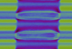
The colorized graphic above shows data collected as the SCM tip rastered across a p/n junction, a common semiconductor structure. Blue and purple areas indicate areas in the junction with low concentrations of the dopant phosphorus, while yellow/green areas have higher concentrations of the dopant boron.
NIST researchers spent three years improving the SCM's spatial resolution and developing computer models based on first principals of physics that translate capacitance signals into two- or three-dimensional, quantitative data on dopant concentrations. They now are creating a database of experimental measurements and modeling predictions to help instrument makers ensure the reliability of quantitative measurements.
Contact: Joe Kopanski, (301) 975-2089. Email: kopanski@sed.eeel.nist.gov.
Atom Lithography May Shrink "Chips"
A new approach to microlithography that uses neutral atoms instead of light to produce patterns in silicon has been demonstrated at NIST by scientists from Harvard University and NIST. The new method offers the promise of one day manufacturing integrated circuits or other microfabricated objects about 10 times smaller than is possible with light-based lithography methods.
The scientists' results are reported in the Sept. 1 issue of the journal Science. Funding for the project was provided by the National Science Foundation and NIST.
Current semiconductor lithography involves shining short wavelength visible or ultraviolet light through detailed masks (stencils) of circuit patterns onto silicon coated with a photosensitive "resist." Areas exposed to the light are damaged and then selectively removed (etched) with chemicals. The smallest circuit linewidths possible with light-based lithography are on the order of 100 to several hundred nanometers.
The new technique uses "metastable" gas atoms instead of light and a resist layer only one molecule thick, much thinner than a typical photoresist. The metastable atoms carry stored energy in the form of excited electrons. When the atoms hit the resist they release their energy, damaging bonds in the molecules. The damaged areas then are chemically etched, leaving unexposed areas unchanged. The new approach provides a much sharper "writing tool" than light waves, which are many times wider than the molecules in the resist.
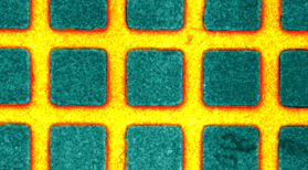
To test the feasibility of the method, the scientists used a copper screen as a mask to etch a grid of gold lines a few micrometers wide with extremely sharp edges (less than 100 nanometers of roughness.) (See colorized graphic above).
Ultimately, the group plans to replace the physical screen in their experiments with a mask created with laser light waves. A pattern of intersecting laser light in the path of a beam of metastable atoms acts like a stencil exposing some areas to damage while protecting other areas. Such a system may produce features only tens of nanometers wide.
Contact: Steven Rolston, (301) 975-6581, email: rolston@enh.nist.gov or Mara Prentiss, (617) 496-5967, email: mara@atomsun.harvard.edu.
Making Tall Spaces More Fire Safe
 High-ceiling areas such as aircraft hangars, hotel atriums, and warehouses
pose some of the most difficult fire safety challenges. Existing building and fire
codes provide little or no guidance on fire protection systems for such tall
structures due to a lack of scientific data.
High-ceiling areas such as aircraft hangars, hotel atriums, and warehouses
pose some of the most difficult fire safety challenges. Existing building and fire
codes provide little or no guidance on fire protection systems for such tall
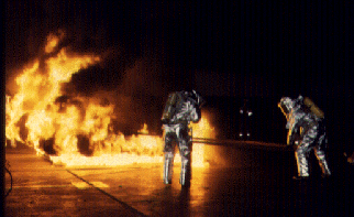
structures due to a lack of scientific data. NIST researchers are working with the U.S. Naval Facilities Engineering Command and five manufacturers from the automatic fire alarm and sprinkler industry in an effort to develop information needed to design fire safety plans specifically for high-ceiling structures. A research team assembled by the cooperating organizations conducted 35 full-scale experiments in two Navy aircraft hangars located in Hawaii and Iceland. (See photo above).
Data were collected on the movement of smoke and heat in two high bay hangars for a variety of fire sizes, using various jet aviation fuels, and with both open and closed hangar doors. The tests also included evaluation of prototype fire detection and suppression methodologies and equipment. Results from the study will be compared with predictions made by three-dimensional computer models under development at NIST with funding from the National Aeronautics and Space Administration.
Contact: Darren Lowe, (301) 975-6667, email:dlowe@enh.nist.gov.
Better Metalmaking Through Modeling
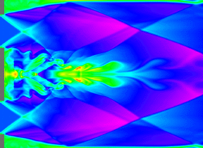 This picture is :
a. a psychedelic Rorschach test.
b. a piece of abstract art.
c. a tool for making jet turbine blades more efficiently.
If you answered "c," you have probably read this newsletter before, and you're right.
The graphic is a tool to better understand high-tech processes for making fine metal powders in a machine called an atomizer. Such powders are pressed and sintered into complex forms, like turbine blades and prosthetic devices, with little or none of the machining required with traditional metal casting.
Generated with a new NIST-developed computer model, the graphic shows a simulated temperature profile for the air in the wake of a speeding bullet. ( Red represents the hottest air, followed by yellow, green, blue, and purple.)
Air flow behind a bullet is a well-studied fluid dynamics problem, supported by extensive data from experiments. By successfully simulating the complex temperature profile for a bullet's wake, NIST researchers are validating the accuracy of their computer model so it can be applied to a similar situation -- gas flow inside a metal atomizer. In the first case, high-speed metal rushes through air. In the metal atomizer, high-speed gas rushes past a liquid metal stream to break it into droplets and form fine powders. Understanding the details of air flow inside metal atomizers should help improve the yield of usable metal powder manufactured, which typically is only about 50 percent.
Contact: Pedro Espina, (301) 975-6178, email: espina@fluid.nist.gov.
New Catalog Lists Reference Data
The latest information on nearly 100 computerized databases and published data compilations available from NIST and other sources is included in the new NIST Standard Reference Data Products Catalog, 1995-1996 Edition (SP 782.) The NIST Standard Reference Data Program provides reliable, well-documented data to scientists and engineers for problem solving, research, and development.Data compilations are available in the following areas: analytical chemistry, atomic and molecular physics, biotechnology, chemical and crystal structure, chemical kinetics, industrial fluids and chemical engineering, materials properties, surface data, thermodynamics and thermochemistry, and special databases of binary images and structured forms.
To obtain a copy of SP 782, send a self-addressed mailing label to: SRDP, A320 Physics Bldg., NIST, Gaithersburg, Md. 20899-0001; (301) 975-2208. The catalog is also available through the World Wide Web at http://www.srd.nist.gov:8231.
Shorts
ATP Helps Zap Bugs Au Naturel
 You can't fool Mother Nature, but it's getting easier to imitate her. A NIST
Advanced Technology Program project completed this summer by AgriDyne
Technologies Inc., Salt Lake City, Utah, has synthesized successfully a natural
insecticide produced by certain chrysanthemum flowers. The flowers, a special
variety of the florist shop favorite, grow best only in Kenya and other east African
nations. Pyrethrins, a family of compounds produced by the flowers, kill insects on
contact. But unlike many synthetic insecticides, pyrethins have low toxicity for
mammals, degrade quickly, and produce no harmful residues. AgriDyne's three-year, cost-shared ATP project proved the technical feasibility of a complex genetic
engineering process for artificially producing pyrethins. The process involved
implanting a flower gene into yeast cells, so that the yeast would produce quantities
of chrysanthemyl alcohol, the critical component needed for synthesizing pyrethins.
With successful field and toxicity testing funded by the company, the insecticide
could be on the market in two to three years. Contact: David Clark, (801) 467-4100.
You can't fool Mother Nature, but it's getting easier to imitate her. A NIST
Advanced Technology Program project completed this summer by AgriDyne
Technologies Inc., Salt Lake City, Utah, has synthesized successfully a natural
insecticide produced by certain chrysanthemum flowers. The flowers, a special
variety of the florist shop favorite, grow best only in Kenya and other east African
nations. Pyrethrins, a family of compounds produced by the flowers, kill insects on
contact. But unlike many synthetic insecticides, pyrethins have low toxicity for
mammals, degrade quickly, and produce no harmful residues. AgriDyne's three-year, cost-shared ATP project proved the technical feasibility of a complex genetic
engineering process for artificially producing pyrethins. The process involved
implanting a flower gene into yeast cells, so that the yeast would produce quantities
of chrysanthemyl alcohol, the critical component needed for synthesizing pyrethins.
With successful field and toxicity testing funded by the company, the insecticide
could be on the market in two to three years. Contact: David Clark, (801) 467-4100.
Aging Silk with Radiation
Repairing and restoring ancient art is an art form itself. The field recently got a small boost from NIST radiation specialists, working cooperatively with conservation experts from the Smithsonian's Freer Gallery of Art in Washington, D.C. The gallery maintains an extensive collection of Chinese, Japanese, and Korean art works painted on silk, many of which are 500 to 1,000 years old. The natural aging process causes deterioration of the silk, producing holes in priceless art works that must be patched as unobtrusively as possible. With a method first used in Japan, NIST scientists irradiated a number of samples of new silk with gamma rays and electrons to find the right dose to accelerate the silk's aging process. They found that very high doses (100,000 higher than the mean lethal human dose) weakened the silk to the right strength and flexibility to match closely the ancient silk scrolls in need of patching. Contact: William McLaughlin, (301) 975-5559.
An Environmentally Friendly Clean
Many industrial processes require the use of solvents to clean a product's surfaces during processing. Unfortunately, a number of industrial solvents bring environmental costs with their benefits. One solvent in particular, 1,1,1-trichloroethane (TCA), will be banned worldwide at the end of 1995 because of its contribution to ozone depletion. The Pollution Prevention Center, Santa Monica, Calif. (a NIST Manufacturing Extension Partnership center), helps small and medium-sized companies find alternatives to TCA and other environmentally hazardous chemicals. Often this means water-based solvents that pose fewer environmental problems. For at least one company the solution was a non-stick coating for its equipment so that it no longer needed regular cleaning. The center was even able to help the movie industry. The staff found a new solvent that cleans fragile movie film as effectively as TCA but with far fewer environmental drawbacks. Contact: Katy Wolf, (310) 453-0450.
Carbon Dating Comes of Age
 For the last two decades NIST scientsts have pioneered use of carbon-14
dating to identify sources of air pollution. Carbon generated in the burning of
contemporary (living) things like wood contains a high percentage of naturally
occurring radioactive carbon-14. Fossil fuels used in industrial boilers or cars
contain little or no carbon 14. By analyzing the percentage of carbon-14 in fine
particles or gases collected from urban air, scientists can estimate the proportion of
air pollution from fossil fuels versus other sources. NIST researchers determined
that fossils fuels were the dominant source of particulate carbon for samples
collected in Denver and of carbon monoxide in Albuquerque. In Los Angeles, about
30 percent of atmospheric, particulate carbon came from contemporary sources.
Inventories of local pollution sources indicate that during non-winter months more
than half of this contemporary carbon comes from charbroiling of meat, while
woodburning was the major source in winter. Such information aids local
governments in establishing pollution control strategies. Contact: Lloyd Currie,
(301) 975-3919, email: currie@enh.nist.gov.
For the last two decades NIST scientsts have pioneered use of carbon-14
dating to identify sources of air pollution. Carbon generated in the burning of
contemporary (living) things like wood contains a high percentage of naturally
occurring radioactive carbon-14. Fossil fuels used in industrial boilers or cars
contain little or no carbon 14. By analyzing the percentage of carbon-14 in fine
particles or gases collected from urban air, scientists can estimate the proportion of
air pollution from fossil fuels versus other sources. NIST researchers determined
that fossils fuels were the dominant source of particulate carbon for samples
collected in Denver and of carbon monoxide in Albuquerque. In Los Angeles, about
30 percent of atmospheric, particulate carbon came from contemporary sources.
Inventories of local pollution sources indicate that during non-winter months more
than half of this contemporary carbon comes from charbroiling of meat, while
woodburning was the major source in winter. Such information aids local
governments in establishing pollution control strategies. Contact: Lloyd Currie,
(301) 975-3919, email: currie@enh.nist.gov.
Co-op Corner
Dental Products -- SmithKline Beecham Corp., Philadelphia, a leading manufacturer of health care products, has licensed several tooth remineralization and desensitization applications from the American Dental Association Health Foundation. ADAHF is located at NIST. The license agreement gives SmithKline Beecham rights to develop and market topical application products based on amorphous calcium phosphate compounds patented by the ADAHF. These compounds make teeth less sensitive and increase resistance to dental caries by filling in microscopic holes and repairing early cavities. When applied in a carbonate solution, the compounds form rapidly and then crystallize to apatite, the mineral in teeth. Contact: Ming Tung, (301) 975-6823, email: tung@enh.nist.gov.
Auto Emissions -- Automakers need new chemical measurement technologies and standards to design cars and trucks that will meet increasingly stringent federal Clean Air requirements and California emission standards. NIST is collaborating with the American Industry Government Emissions Research organization to help U.S. auto manufactuers develop and test low-emission vehicles. AIGER includes U.S. automakers (Chrysler, Ford, General Motors, and Navistar), the California Air Resources Board, and the Environmental Protection Agency. The effort will include development of new exhaust emissions analysis technologies and standards based on microsensor arrays, infrared light, and microwaves. Contact: Willie May, (301) 975-3108, email: wem@micf.nist.gov.
Data Storage -- Optical tape is an emerging media for high-density storage of computer data. NIST researchers are participating in the Optical Tape Study Group established by the Association for Information and Image Management International to help industry develop measurements, evaluation techniques, and specifications for long-term computer data storage with optical tape. The study group explores such issues as data integrity, metrology concerns, media and drive specifications, and possible future standards. Several key organizations from industry and government participate in the study group. Contact: Fernando Podio, (301) 975-2947, email: fernando@pegasus.ncsl.nist.gov.
Crack Detection -- NIST scientists have developed a practical wide-band acoustic emission sensor for detecting cracks in steel bridges, pressure vessels, and composite parts, such as those used in automobiles and aircraft. The new sensor features a significant increase in sensitivity that rivals the level found in narrow-band resonant sensors. Under a cooperative agreement with DECI, a company in San Juan Capistrano, Calif., the researchers hope to combine the best elements of the NIST sensor and a similar device developed by the private firm. For a copy of paper no. 19-95 describing this work, contact Sarabeth Harris, (303) 497-3237, email:smoynihan@micf.nist.gov.
About Technology at a Glance:
NIST is an agency of the U.S. Department of Commerce's Technology Administration. NIST promotes U.S. economic growth by working with industry to develop and apply technology, measurements, and standards. Technology at a Glance is produced by the Public and Business Affairs Division, A903 Administration Bldg., NIST, Gaithersburg, Md. 20899-0001. Any mention of commercial products is for information only; it does not imply recommendation or endorsement by NIST. Technology at a Glance Editor: Gail Porter, (301) 975- 3392, email:gail.porter@nist.gov. For patent information, call (301) 975-3084.
