| June 24, 2008

[NIST Tech Beat Search] [Credits] [NIST Tech Beat Archives] [Media Contacts] [Subscription Information]

New Process Creates 3-D Nanostructures with Magnetic Materials
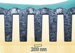 |
Working in the trenches: Transmission electron microscopy image of a thin cross section of 160 nanometer trenches shows deposited nickel completely filling the features without voids. (Color added for clarity.)
Credit: NIST
View hi-resolution image |
Materials scientists at the National Institute of Standards and Technology (NIST) have developed a process to build complex, three-dimensional nanoscale structures of magnetic materials such as nickel or nickel-iron alloys using techniques compatible with standard semiconductor manufacturing. The process, described in a recent paper,* could enable whole new classes of sensors and microelectromechanical (MEMS) devices.
The NIST team also demonstrated that key process variables are linked to relatively quick and inexpensive electrochemical measurements, pointing the way to a fast and efficient way to optimize the process for new materials.
The NIST process is a variation of a technique called “Damascene metallization” that often is used to create complicated three-dimensional copper interconnections, the “wiring” that links circuit elements across multiple layers in advanced, large-scale integrated circuits. Named after the ancient art of creating designs with metal-in-metal inlays, the process involves etching complex patterns of horizontal trenches and vertical “vias” in the surface of the wafer and then uses an electroplating process to fill them with copper. The high aspect ratio features may range from tens of nanometers to hundreds of microns in width. Once filled, the surface of the disk is ground and polished down to remove the excess copper, leaving behind the trench and via pattern.
The big trick in Damascene metallization is ensuring that the deposited metal completely fills in the deep, narrow trenches without leaving voids. This can be done by adding a chemical to the electrodeposition solution to prevent the metal from building up too quickly on the sides of the trenches and by careful control of the deposition process, but both the chemistry and the process variables turn out to be significantly different for active ferromagnetic materials than for passive materials like copper. In addition to devising a working combination of electrolytes and additives to do Damascene metallization with nickel and a nickel-iron alloy, the NIST team demonstrated straightforward measurements for identifying and optimizing the feature-filling process thereby providing an efficient path for the creation of quality nanoscale ferromagnet structures.
The new process makes it feasible to create complex three-dimensional MEMS devices such as inductors and actuators that combine magnetic alloys with non-magnetic metallizations such as copper interconnects using existing production systems.
* C.H. Lee, J.E. Bonevich, J.E. Davies and T.P. Moffat. Magnetic materials for three-dimensional Damascene metallization: void-free electrodeposition of Ni and Ni70Fe30 using 2-mercapto-5-benzimidazolesulfonic acid. Journal of The Electrochemical Society, 155 (7) D499-D507 (2008).
Media Contact: Michael Baum, michael.baum@nist.gov, (301) 975-2763 
Exposing the Sensitivity of Extreme Ultraviolet Photoresists
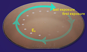 |
NIST researchers exposed a 300 mm silicon wafer with incrementally increasing doses of extreme ultraviolet light (EUV) in 15 areas. After the wafer was developed, the team determined that the seventh exposure was the minimum dose required (E0) to fully remove the resist.
Credit: NIST
View hi-resolution image |
Researchers at the National Institute of Standards and Technology (NIST) have confirmed that the photoresists used in next-generation semiconductor manufacturing processes now under development are twice as sensitive as previously believed. This finding, announced at a workshop last month,* has attracted considerable interest because of its implications for future manufacturing. If the photoresists are twice as sensitive as previously thought, then they are close to having the sensitivity required for high volume manufacturing, but the flip side is that the extreme ultraviolet optical systems in the demonstration tools currently being used are only about half as effective as believed.
Extreme ultraviolet lithography (EUVL) is a process analogous to film photography. A silicon wafer is coated with photoresist and exposed to EUV light that reflects off a patterned “photomask.” Where the light strikes the resist it changes the solubility of the coating. When developed, the soluble portions wash away leaving the same pattern exposed on the silicon surface for the processing steps that ultimately create microcircuits.
The drive to make circuits with ever smaller features has pushed manufacturers to use shorter and shorter wavelengths of light. EUVL is the next step in this progression and requires developing both suitable light sources and photoresists that can retain the fine details of the circuit, balancing sensitivity, line edge roughness and spatial resolution. NIST researcher Steve Grantham says that optical lithography light sources in use today emit light with a wavelength of about 193 nanometers, which borders on optical wavelengths. EUVL sources produce light with wavelengths about an order of magnitude smaller, around 13.5 nanometers. Because this light does not travel through anything—including lenses—mirrors have to be used to focus it.
Until recently, EUV photoresist sensitivity was referenced to a measurement technique developed at Sandia National Labs in the 1990s. Late in 2007, scientists at the Advanced Light Source at Lawrence Berkeley National Laboratory in Berkeley, Calif., used a NIST-calibrated photodetector to check the standard. Their detector-based measurements indicated that the resist’s sensitivity was about twice that of the resist-based calibration standard.
Following on the intense interest that these results generated when the Berkeley group presented them at a conference in February, the Intel Corporation asked scientists at NIST to make their own independent determination of the EUVL resist sensitivity to validate the results. Measurements conducted at the NIST SURF III Synchrotron Ultraviolet Radiation Facility agreed with those of the Berkeley group. The fact that the photoresist is now known to be twice as sensitive to the EUV light implies that half as much light energy as had been expected is arriving at the wafer.
“These results are significant for a technology that faces many challenges before it is slated to become a high-volume manufacturing process in 2012,” Grantham says. “It should open the eyes of the industry to the need for accurate dose metrology and the use of traceable standards in their evaluations of source and lithography tool performance.”
* S. Grantham, C. Tarrio, R. E. Vest, T. B. Lucatorto, A. Novembre, M. Cangemi, V. Prabhu, K.W. Choi, M. Chandhok, T. Younkin and J. S. Clarke. SEMATECH EUV Source Workshop, Bolton Landing, N.Y., May 12, 2008.
Media Contact: Mark Esser, mark.esser@nist.gov, (301) 975-8735
‘Electron Trapping’ May Impact Future Microelectronics Measurements
Using an ultra-fast method of measuring how a transistor switches from the “off” to the “on” state, researchers at the National Institute of Standards and Technology (NIST) recently reported that they have uncovered an unusual phenomenon that may impact how manufacturers estimate the lifetime of future nanoscale electronics.
The transistor is one of the basic building blocks of modern electronics, and the life expectancy or reliability of a transistor is often projected based on the response to an accelerated stress condition. Changes in the transistor’s threshold voltage (the point at which it switches on) are typically monitored during these lifetime projections. The threshold voltage of certain types of transistors (p-type) is known to shift during accelerated stresses involving negative voltages and elevated temperatures, a characteristic known as “negative bias temperature instability” (NBTI). This threshold voltage shift recovers to varying degrees once the stress has ended. This “recovery” makes the task of measuring the threshold voltage shift very challenging and greatly complicates the prediction of a transistor’s lifetime.
As semiconductor devices reach nanoscale (billionth of a meter) dimensions, measuring this device reliability accurately becomes more important because of new materials, new structures, higher operating temperatures and quantum mechanical effects. Many NBTI studies show that the accuracy of the measured threshold voltage shift (and consequent accuracy of the lifetime prediction) depends strongly on how quickly the threshold voltage can be measured after the stress is finished. So, NIST engineers began making threshold voltage measurements at very fast speeds, leaving as little as two microsceconds (millionths of a second) between measurements instead of the traditional half-second interval. What they observed was surprising.
“We found that NBTI recovery not only returned the threshold voltage to its pre-stressed state but briefly passed this mark and temporarily allowed the transistor to behave better than the pre-stressed state,” says Jason Campbell, a member of the NIST team (that includes Kin Cheung and John Suehle) who presented this finding at the recent Symposium on VLSI Technology in Hawaii. The NBTI effect generally is believed to result from the buildup of positive charges, he explained, but the new observations at NIST indicate the presence of negative charge as well. NIST’s ultra-fast and ultra-sensitive measurements revealed that during recovery, the positive charges dissipated faster than the electrons, giving the system a momentary negative charge and heightened conductivity.
To date, Campbell says, transistor manufacturers only consider the accumulation of positive charges to predict the longevity of their microelectronics devices. “But as these systems get smaller and smaller, the electron trapping phenomenon we observed will need to be considered as well to ensure that transistor lifetime predictions stay accurate,” he says. “Our research will now focus on developing and refining the ability to measure that impact.”
Media Contact: Michael E. Newman, michael.newman@nist.gov, (301) 975-3025
Oxygen Ions for Fuel Cells Get Loose at Low(er) Temperatures
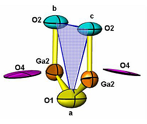 |
Researchers determined that a new material for fuel cells releases oxygen ions easily at low temperatures because many of the oxygen ions—marked here as O4—are not closely bound to the material's crystal framework.
Credit: X. Kuang, University of Liverpool |
Seeking to understand a new fuel cell material, a research team working at the National Institute of Standards and Technology (NIST), in collaboration with the University of Liverpool, has uncovered a novel structure that moves oxygen ions through the cell at substantially lower temperatures than previously thought possible. The finding announced this month in Nature Materials may be key to solving fuel cell reliability issues and lead to reduced operating costs in high-performance stationary fuel cells.
Electricity is produced in fuel cells from the electrochemical reaction between a hydrogen-rich fuel and oxygen that produces electric current and water. Research on small fuel cells for cars has dominated the news, but stationary fuel cells are the Goliaths—operating at up to 70 percent efficiency and providing enough electricity—up to 100 megawatts—to power small cities, hospitals, military installations or airports without relying on the electric power grid. Smaller versions are being considered for auxiliary power units in such applications as refrigeration trucks to reduce engine idling.
They are called “solid oxide” fuel cells (SOFCs) because the heart of the cell is a solid electrolyte that transports oxygen ions extracted from air to meet with hydrogen atoms. This alchemy traditionally requires high temperatures—about 850 degrees Celsius in conventional SOFCs—and therefore long startup times, ranging from 45 minutes to eight hours.
The high temperatures necessitate more expensive materials and higher operating costs, so stationary fuel cell research is focused on lowering operating temperatures as well as shortening startup times. The U.S. Department of Energy’s goal is to slash the startup time to two minutes.
Chemists at the University of Liverpool fabricated a new oxygen ion electrolyte material of lanthanum, strontium, gallium and oxygen and sent it to the NIST Center for Neutron Research (NCNR) to investigate with collaborators from NIST, the University of Maryland and University College London. Neutrons provide an atomic-scale view of materials so scientists can “see” what is happening at that level.
The oxygen ions in the new materials become mobile at 600 degrees C, much lower than previously studied materials. Researchers suspected the reason lay in the location of the oxygen ions in the crystal framework of the compound. The neutron probes allowed them to determine the basic crystal structure that held the lanthanum, strontium, gallium and oxygen atoms, however the exact nature of the extra oxygen ions was unclear.
NCNR researchers recommended borrowing a method from radio astronomy called maximum entropy analysis. “When astronomers are not able to visualize a specific part of an image because it constitutes such a small part of the total information collected, they utilize a part of applied mathematics called information theory to reconstruct a sharper image,” explains NCNR researcher Mark Green. “The combination of neutron diffraction and maximum entropy analysis not only allowed us to determine the location of additional oxygen ions outside of the basic framework, but revealed a new mechanism for ion conduction.”
“It allows us to take a fundamentally different approach in the design of future materials, so that we can harness this new mechanism for oxide ion conduction and produce lower operating fuel cells,” says Green. “This type of work is very important to us, which is why as part of the NCNR expansion we are developing a new materials diffractometer that will greatly enhance our capabilities in energy related research.”
* X. Kuang, M.A. Green, H. Niu, P Zajdel, C. Dickinson, J.B. Claridge, L. Jantsky and M.J. Rosseinsky. Interstitial oxide ion conductivity in the layered tetrahedral network melilite structure. Nature Materials, June 2008
Media Contact: Evelyn Brown, evelyn.brown@nist.gov, (301) 975-5661
Standards Set for Energy-Conserving LED Lighting
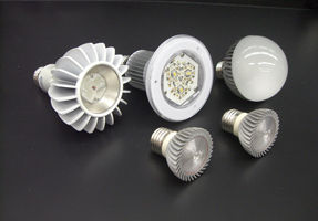 |
These solid-state lights are powered by energy-efficient light emitting diodes and are among the first ones of a new generation expected to cut energy needed for lighting by 50 percent by 2027.
Credit: NIST
View hi-resolution image |
Scientists at the National Institute of Standards and Technology (NIST), in cooperation with national standards organizations, have taken the lead in developing the first two standards for solid-state lighting in the United States. This new generation lighting technology uses light-emitting diodes (LEDs) instead of incandescent filaments or fluorescent tubes to produce illumination that cuts energy consumption significantly.
Standards are important to ensure that products will have high quality and their performance will be specified uniformly for commerce and trade. These standards—the most recent of which published last month—detail the color specifications of LED lamps and LED light fixtures, and the test methods that manufacturers should use when testing these solid-state lighting products for total light output, energy consumption and chromaticity, or color quality.
Solid-state lighting is expected to significantly reduce the amount of energy needed for general lighting, including residential, commercial and street lighting. “Lighting,” explains NIST scientist Yoshi Ohno, “uses 22 percent of the electricity and 8 percent of the total energy spent in the country, so the energy savings in lighting will have a huge impact.”
Solid-state lighting is expected to be twice as energy efficient as fluorescent lamps and 10 times more efficient than incandescent lamps, although the current products are still at their early stages. Ohno chaired the task groups that developed these new standards.
In addition to saving energy, the new lighting, if designed appropriately, can produce better color rendering—how colors of objects look under the illumination—than fluorescent lamps or even incandescent lamps, Ohno says.
NIST is working with the U.S. Department of Energy (DOE) to support its goal of developing and introducing solid-state lighting to reduce energy consumption for lighting by 50 percent by the year 2025. The department predicts that phasing in solid-state lighting over the next 20 years could save more than $280 billion in 2007 dollars.
The Illuminating Engineering Society of North America (IESNA) published a documentary standard LM-79, which describes the methods for testing solid-state lighting products for their light output (lumens), energy efficiency (lumens per watt) and chromaticity. Details include the environmental conditions for the tests, how to operate and stabilize the LED sources for testing and methods of measurement and types of instruments to be used.
“More standards are needed, and this will be the foundation for all solid-state lighting standards,” Ohno says. The standard is available from the IESNA.
The solid-state lights being studied are intended for general illumination, but white lights used today vary greatly in chromaticity, or specific shade of white. The American National Standards Institute (ANSI) published the standard C78.377-2008, which specifies the recommended color ranges for solid-state lighting products using cool to warm white LEDs with various correlated color temperatures. The standard may be downloaded from ANSI’s Web site. www.nema.org/stds/ANSI-ANSLG-C78-377.cfm
DOE is launching the Energy Star program for solid-state lighting products this fall. NIST scientists assisted DOE by providing research, technical details and comments for the Energy Star specifications. The Energy Star certification assures consumers that products save energy and are high quality and also serves as an incentive for manufacturers to provide energy-saving products for consumers.
The solid-state lighting community is continuing to develop LED lighting standards for rating LED lamp lifetime and for measuring the performance of the individual high-power LED chips and arrays. NIST scientists are taking active roles in these continuing efforts.
Media Contact: Evelyn Brown, evelyn.brown@nist.gov, (301) 975-5661
NIST Releases Preview of Much-Anticipated Online Mathematics Reference
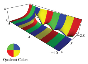 |
This visual representation of a Hankel function for complex variables in the NIST Digital Library of Mathematical Functions can be explored in three dimensions by Web users. Hankel functions are solutions of Bessel's differential equation, and they play an important role in many problems of mathematical physics, such as heat conduction and wave propagation.
Credit: NIST
View hi-resolution image |
The National Institute of Standards and Technology (NIST) has released a five-chapter preview of the much-anticipated online Digital Library of Mathematical Functions (DLMF). In development for over a decade, the DLMF is designed to be a modern successor to the 1964 “Handbook of Mathematical Functions,” a reference work that is the most widely distributed NIST publication (with over a million copies in print) and one of the most cited works in the mathematical literature (still receiving over 1,600 yearly citations in the research literature). The preview of the new DLMF is a fully functional beta-level release of five of the 36 chapters.
The DLMF is designed to be the definitive reference work on the special functions of applied mathematics. Special functions are “special” because they occur very frequently in mathematical modeling of physical phenomena, from atomic physics to optics and water waves. These functions have also found applications in many other areas; for example, cryptography and signal analysis. The DLMF provides basic information needed to use these functions in practice, such as their precise definitions, alternate ways to represent them mathematically, illustrations of how the functions behave with extreme values and relationships between functions.
The DLMF provides various visual aids to provide qualitative information on the behavior of mathematical functions, including interactive Web-based tools for rotating and zooming in on three-dimensional representations. These 3-D visualizations can be explored with free browsers and plugins designed to work in virtual reality markup language (VRML). Mouse over any mathematical function, and the DLMF provides a description of what it is; click on it, and the DLMF goes to an entire page on the function. The DLMF adheres to a high standard for handbooks by providing references to or hints for the proofs of all mathematical statements. It also provides advice on methods for computing mathematical functions, as well as pointers to available software.
The complete DLMF, with 31 additional chapters providing information on mathematical functions from Airy to Zeta, is expected to be released in early 2009. With over 9,000 equations and more than 500 figures, it will have about twice the amount of technical material of the 1964 Handbook. An approximately 1,000-page print edition that covers all of the mathematical information available online also will be published. The DLMF, which is being compiled and extensively edited at NIST, received initial seed money from the National Science Foundation and resulted from contributions of more than 50 subject-area experts worldwide. The NIST editors for the DLMF are Frank W. J. Olver, Daniel W. Lozier, Ronald F. Boisvert and Charles W. Clark.
The DLMF preview can be accessed at http://dlmf.nist.gov/.
Media Contact: Ben Stein, bstein@nist.gov, (301) 975-3097
Micromagnets Show Promise as Colorful ‘Smart Tags’ for MRI
 |
 |
Microscopic magnets (above left), designed and tested in a joint NIST/NIH project, might one day be injected into the body to add color and “smart tag” capability to magnetic resonance imaging for medical diagnosis and research. The image on the right shows light scattering from grids of magnets on a wafer where they were made using conventional microfabrication techniques.
Credit: NIST
View hi-resolution of image on left | View hi-resolution of image on right |
Customized microscopic magnets might one day be injected into the body to add color to magnetic resonance imaging (MRI) while enhancing sensitivity and the amount of information provided by images researchers at the National Institute of Standards and Technology (NIST) and National Institutes of Health (NIH) report. The new micromagnets also could act as “smart tags,” identifying particular cells, tissues or physiological conditions for medical research or diagnostic purposes.
As described in the June 19 issue of Nature,* the NIST and NIH investigators have demonstrated the proof of principle for a new approach to MRI. Unlike the chemical solutions now used as image-enhancing contrast agents in MRI, the NIST/NIH micromagnets rely on a precisely tunable feature—their physical shape—to adjust the radiofrequency (RF) signals used to create images. The RF signals then can be converted into a rainbow of optical colors by computer. Sets of different magnets designed to appear as different colors could, for example, be coated to attach to different cell types, such as cancerous versus normal.
“Current MRI technology is primarily black and white; this is like a colored tag for MRI,” says lead author Gary Zabow, who designed and fabricated the microtags at NIST and, together with colleagues at the National Institute of Neurological Disorders and Stroke, part of NIH, tested them on MRI machines.
The microtags would need extensive further engineering and testing, including clinical studies, before they could be used in people. The initial prototypes were made of nickel, which is toxic but relatively easy to work with, but Zabow says they could be made of other magnetic materials, such as iron, which is considered non-toxic and is already approved for use in certain medical agents. Only very low concentrations of the magnets would be needed in the body to enhance MRI images.
Each micromagnet consists of two round vertically stacked magnetic discs a few micrometers in diameter separated by a small open gap in between. Researchers create a customized magnetic field for each tag by making it from particular materials and tweaking the geometry, perhaps by widening the gap between the discs or changing the discs’ thickness or diameter. As water in a sample flows between the discs, protons acting like twirling bar magnets within the water’s hydrogen atoms generate predictable RF signals—the stronger the magnetic field, the faster the twirling—and these signals are used to create images. The magnets could make medical diagnostic images as information-rich as the optical images of tissue samples now common in biotechnology, which already benefits from a variety of colored markers such as fluorescent proteins and tunable quantum dots.
NIH support for Zabow’s work was funded by the National Institute of Biomedical Imaging and Bioengineering (NIBIB) through the NIST/NIH-NIBIB National Research Council Joint Associateship Program. NIH has filed a provisional patent application on the micromagnets.
To read more about micromagnets, see “NIST/NIH Micromagnets Show Promise as Colorful ‘Smart Tags’ for Magnetic Resonance Imaging.”
* G. Zabow, S. Dodd, J. Moreland, A. Koretsky. 2008. Micro-engineered local field control for high-sensitivity multispectral MRI. Nature. June 19.
Media Contact: Laura Ost, laura.ost@nist.gov, (303) 497-4880
Physicists Produce Quantum-Entangled Images
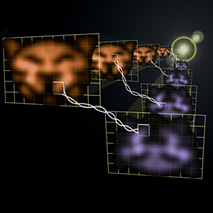 |
In this photo montage of actual quantum images, two laser beams coming from the bright glare in the distance transmit images of a cat-like face at two slightly different frequencies (represented by the orange and the purple colors). The twisted lines indicate that the seemingly random changes or fluctuations that occur over time in any part of the orange image are strongly interconnected or “entangled” with the fluctuations of the corresponding part in the purple image. Though false color has been added to the cats’ faces, they are otherwise actual images obtained in the experiment.
Credit: NIST
View hi-resolution image |
Using a convenient and flexible method for creating twin light beams, researchers from the National Institute of Standards and Technology (NIST) and the University of Maryland (UM) have produced “quantum images,” pairs of information-rich visual patterns whose features are “entangled,” or inextricably linked by the laws of quantum physics.
In addition to promising better detection of faint objects and improved amplification and positioning of light beams, the researchers’ technique for producing quantum images—unprecedented in its simplicity, versatility, and efficiency—may someday be useful for storing patterns of data in quantum computers and transmitting large amounts of highly secure encrypted information. The research performed at the NIST/UM Joint Quantum Institute (JQI) was described in the June 12 edition of Science Express.*
Conventional photographic films or digital camera sensors only record the color and intensity of a light wave striking their surfaces. A hologram additionally records a light wave’s “phase”—the timing the crests and valleys in the wave. However, much more happens in a light wave. Even the most stable laser beam brightens and dims randomly over time because light has inherent quantum level “uncertainties” in its properties. Controlling these fluctuations—which represent a sort of “noise”—can improve detection of faint objects, produce better amplified images and allow workers to more accurately position laser beams. Researchers can’t completely eliminate the noise, but they can rearrange it to improve desired features in images. A quantum-mechanical technique called “squeezing” lets physicists reduce noise in one property—such as intensity—at the expense of increasing the noise in a complementary property, such as phase. In addition to noise reduction, the quantum manipulations open new applications for images—such as transferring heaps of encrypted data protected by the laws of quantum mechanics and performing parallel processing of information for quantum computers.
The quantum images produced by the JQI team are in “entangled” pairs, transmitted by two light beams originating from the same point. Look at one quantum image, and it displays random and unpredictable changes over time. Look at the other image, and it exhibits very similar random fluctuations at the same time, even if the two images are far apart and unable to transmit information to one another. Together, they are squeezed: Matching up both quantum images and subtracting their fluctuations, their noise is lower—and their information content potentially higher—than it is from any two classical images. Each image is made of up to 100 distinct regions, akin to the pixels forming a digital image, each with its own independent optical and noise properties. A pixel on one image forms a partnership with a pixel on the other image—one could predict many of the properties in the second pixel just by looking at the first.
Previous efforts at making quantum images have been limited to building them up with “photon counting”—collecting one photon at a time over a long period of time—or having very specialized “images” such as something that could only be constructed from a dot and a ring. In contrast, the new method produces an entire image at one time and can make a wide variety of images in any shape. A next goal for the researchers is to produce quantum images with slowed-down light; such slowed images could be used in information storage and processing as well as communications applications.
For more details, read “Physicists Produce Quantum-Entangled Images”.
* V. Boyer, A. Marino, R. Pooser, and P. Lett. Entangled Images from Four-Wave Mixing. To Appear in Science Express, 12 June 2008.
Media Contact: Ben Stein, bstein@nist.gov, (301) 975-3097
Quick Links
High Rise Fire Fighting—Effective Use of Positive Pressure Ventilation
National Institute of Standards and Technology (NIST) engineers recently released a two-disk DVD set that demonstrates how Positive Pressure Ventilation (PPV), a technique in which powerful fans force smoke and heat from corridors and stairwells, can increase the effectiveness of firefighters and survivability of occupants in high rise structures.
The DVD collection of PPV videos, reports and a narrated slide presentation are the result of more than six years of NIST PPV experiments and computer simulations. A user-friendly graphic menu allows simple access to all the videos of the high-rise experiments. Users can select single and multi-camera views of events in the rooms of the different apartments. The multimedia presentations as well as the extensive discussion of appropriate PPV techniques for different high-rise building fires makes the DVD set a useful tool for firefighter training.
NIST’s PPV work has been supported by the Department of Homeland Security Science and Technology Directorate and the United States Fire Administration, as well as fire departments across the country. The DVD set, titled “Positive Pressure Ventilation Research: Videos & Reports” by Stephen Kerber and Daniel Madrzykowski, is free. To receive a copy, send a request with a name and mailing address via e-mail to Yalasha Redd at yalasha.redd@nist.gov or Steve Kerber at skerber@nist.gov.
2008-2009 Commerce Science and Technology Fellows Announced
Commerce Secretary Carlos M. Gutierrez today announced that 17 individuals have been selected to participate in the Commerce Science and Technology Fellowship (ComSci) Program. Established in 1964 and later enacted by Congress, ComSci is a 10-month policy study and leadership program that is open to career senior federal employees from any government agency. The ComSci Program takes its participants behind the scenes to learn about science and technology policy-making and management from the brightest minds in government, industry and academia.
“This year marks the induction of the 40th class of ComSci Fellows,” said Gutierrez. “The individuals selected to participate in this esteemed program will have the opportunity to gain an in-depth knowledge of the intricacies of science and technology policy at the national and international levels. The insights that ComSci Fellows pass on have and will continue to ensure that the technical and scientific leadership of the United States will endure.”
For a list of the 2008-2009 ComSci Fellows see “Commerce Secretary Gutierrez Announces Selection of 2007-2008 Commerce Science and Technology Fellows.”
For more information on the ComSci program, go to www.comsci.gov.
|