| January 8, 2008

[NIST Tech Beat Search] [Credits] [NIST Tech Beat Archives] [Media Contacts] [Subscription Information]

Rough Times: NIST's New Approach to Surface Profiling
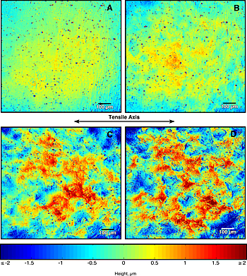 |
The four images (taken with scanning laser confocal microscopy) show variations in surface roughness of an aluminum alloy as produced by increasing amounts of strain: A – 1 percent, B – 4 percent, C – 8 percent and D – 12 percent.
Credit: Mark Stoudt, Joseph Hubbard and Stanley Janet, NIST
View higher resolution image |
Researchers at the National Institute of Standards and Technology (NIST) have developed a novel technique for measuring the roughness of surfaces that is casting doubt on the accuracy of current procedures. Their results announced in a forthcoming paper* could cut development costs for automakers as they design manufacturing tools for new, fuel-efficient, lightweight alloys.
Surface roughness is a key issue for auto manufacturers and other industries that use sheet metal, one that goes far beyond simple cosmetics. Faint striations and other marks that appear when metal is shaped can indicate residual stresses that can cause the part to fail later on. They also lead to extra wear and early retirement for the expensive stamping dies used to form sheet metal into fenders and other body parts (a typical production die can cost $2 million or more.) And measures of surface roughness feed into models that predict friction and the metal’s “springback”—the amount it will unbend after being stamped. Springback has to be known and controlled to build accurate dies for complex metal shapes. A significant cost in introducing new lightweight alloys for cars is the trial-and-error process needed to develop a new set of dies for each new alloy.
Conventionally, roughness is measured with a profilometer, an instrument with a probe like a high-tech phonograph needle that is tracked in a line across the test surface to record the peaks and valleys. The process is repeated several times at intervals across the test surface, and the results are averaged into a “roughness” figure. (New non-contact instruments use optical probes, but the idea is the same.) But NIST researchers have found that these measures may be misleading—as both measurement uncertainties and statistical errors are compounded when the 2-D lines are extrapolated to the entire surface.
NIST’s approach uses data from a scanning laser confocal microscope (SLCM), an instrument that builds a point-by-point image of a surface in three dimensions. The data from a single SLCM image—representing an area of about 1000 X 800 micrometers by 20 micrometers in depth—are analyzed using mathematical techniques that treat every point in the image simultaneously to produce a roughness measure that effectively considers the entire 3-D surface rather than a collection of 2-D stripes.
One early finding is that the generally accepted linear relationship between surface roughness and material deformation is wrong, at least for the aluminum alloy the group studied. The more accurate data from the 3-D analysis shows that a more complicated relationship was masked by the large uncertainties of the linear profilometers. The NIST researchers hope their new technique will lead to more accurate models of the effects of strain on new alloys and, eventually, lower development and tooling costs for metalworking industries.
* M.R. Stoudt, J.B. Hubbard and S.A. Janet. “Using matrix methods to characterize evolution of deformation induced surface roughness in aluminium sheet,” Materials Science and Technology, In Press.
Media Contact: Michael Baum, michael.baum@nist.gov, (301) 975-2763

Radioactive 'Understudy' May Aid Medical Imaging, Drug Development
 |
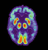 |
Two examples of positron emission tomography (PET) scans. The left image shows a normal brain, the right shows a brain with characteristics of Alzheimer’s disease.
Credit: Alzheimer’s Disease Education and Referral Center, National Institute on Aging |
Broadway stars have understudies. Now, an increasingly popular radioactive isotope has its own stand-in. Developed in part by researchers at the National Institute of Standards and Technology (NIST), the substance might ultimately improve medical imaging, speed up clinical trials of many drugs and facilitate efforts to develop more individualized medical treatment.
The number of medical images obtained through the technique known as positron emission tomography (PET) is increasing at a rate of 20 percent a year—and this has correspondingly increased the use of fluorine-18 (18F), the radioactive isotope of choice in the vast majority of PET procedures. Injected into the bloodstream while bound to “carrier” molecules, fluorine-18 lights up the body during PET scans to perform such jobs as revealing tumors, monitoring heart activity and determining which regions of the brain are active during certain tasks.
However, fluorine-18 has a very short life—a batch of the stuff decays to half its initial quantity in fewer than two hours, and less than one-ten-thousandth of the original amount is left after a single day. Because the stuff decays so quickly, it is not possible for a single central lab to make precise measurements on fluorine-18 solutions and then distribute them to far-flung centers to calibrate PET machines. This lack of a “standard reference” for fluorine-18 means that PET-related measurements from center to center, from patient to patient, and even in the same patient over time, are difficult or impossible to compare with one another.
NIST researchers, collaborating with an Ohio-based nuclear medicine company called RadQual, have turned to germanium-68 (68Ge) as a calibration surrogate for fluorine-18. This germanium isotope is much longer lived—its half-life is 270.95 days—but its radiation decay characteristics are otherwise similar to fluorine-18. Small differences between measurements of germanium-68 and fluorine-18 can be accounted for through the use of mathematical “conversion factors.” Germanium-68 never would be used in actual PET procedures; it would only be used to calibrate the machines properly, enabling more accurate measurements of the fluorine-18 isotopes. Although germanium-68 has been used for performing corrections on PET scanners, the industry has lacked a nationally traceable standard reference material for instrument calibration.
NIST researchers have calibrated solutions of germanium-68 that could become the basis of a new standard reference material for this isotope. The next phase of this project involves working with RadQual to calibrate a new “mock” syringe standard that would use germanium-68 embedded in an epoxy to simulate fluorine-18 in a syringe. This would help researchers more accurately determine the amount of fluorine-18 to be injected into patients during the PET procedure so as to minimize radiation dose while still producing the best image. NIST is also working independently on a 68Ge-based PET “phantom” that can be used to calibrate PET scanners in a way that is traceable back to NIST.
The first commercial products from this collaboration may be reaching PET centers later this year. By giving doctors more accurate results on how specific patients are responding to cancer treatments and providing more precise indications earlier in clinical trials as to how individual patients are metabolizing particular drugs, better standards for PET imaging may hasten the arrival of “individualized” medicine.
Media Contact: Ben Stein, bstein@nist.gov, (301) 975-3097
Measurement Innovations Add Up to Big Savings for Semiconductors
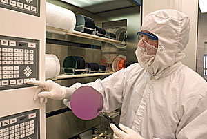 |
Russell Hajdaj prepares silicon wafers that will be "baked" as part of the processing required for producing new types of semiconductor devices.
Credit: Copyright Robert Rathe
View hi-resolution image |
A new report* from the National Institute of Standards and Technology (NIST) shows that investment in measurement science has and will continue to have a dramatic effect on innovation, productivity, growth and competitiveness in and among high technology sectors. Citing the semiconductor industry as a case in point, the analysis, prepared for NIST by RTI International (RTI), estimates that the $12 billion spent on advancing measurement capabilities during the decade beginning in 1996 will have saved that sector more than $51 billion in scrap and rework costs by 2011—a net benefit of approximately $39 billion.
RTI estimates that for every dollar spent on measurement, the industry as a whole saw a $3.30 return. (Dollar amounts represent 2006 dollars adjusted for inflation.) The report found that the strategic focus on measurement technologies pursued by the International Technology Roadmap for Semiconductors (ITRS), a consortium of chip manufacturers and related stakeholders, benefited both the industry and consumers through the reduction of defect rates and the miniaturization of feature size. The advances fostered through this effort, among others, resulted in lower costs, higher product quality and ever faster processing speeds.
Measurement technology has allowed the industry to keep up with “Moore’s Law,” which predicts the number of transistors per chip will double every two years. By the early 1990s, the industry realized it would no longer be possible to satisfy this benchmark without the ability to manipulate nanoscale-sized features. The report credits the initiative to augment nanoscale measurement capabilities outlined in the ITRS and its predecessor as one of the factors that helped manufacturers to increase the possible number of transistors per chip from 3.1 million in 1996 to 1.7 billion in 2006 while making marked improvements in quality, design, software and interoperability.
The report underlines the importance of measurement science to the semiconductor industry and highlights several areas that need further improvement if the industry is to stay on pace. These areas include the need for new standards for measuring features lengths at 32 nanometers, new techniques for controlling radio-frequency electromagnetic energy and high-frequency magnetic fields, and better chemical and materials standards, as well as new and more accurate calibration, interoperability and test standards.
RTI gathered the information for this analysis through surveys and other means. The answered queries accounted for more than 80 percent of the semiconductor industry, and the results were taken to be representative of the industry as a whole. The results may also be viewed as conservative in that RTI was able to quantitatively estimate productivity impacts but not increases in quality.
*Economic Impact of Measurement in the Semiconductor Industry is available on the NIST Web site at http://www.nist.gov/director/planning/policy_studies.htm
Media Contact: Mark Esser, mark.esser@nist.gov, (301) 975-2767
NIST, EC Agency Partner for Better Measurements and Standards
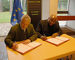 |
Alejandro Herrero, director of the European Commission’s Joint Research Centre Institute for Reference Materials and Measurements (JRC IRMM), and NIST Chemical Science and Technology Laboratory Director Willie May sign a pact in Belgium on Dec. 17, 2007, to advance the development and availability of international measurement standards in the fields of chemistry, life sciences and emerging technologies.
Credit: Doris Florian, JRC IRMM |
Enhancing trade between the United States and the nations of the European Union (EU) while helping ensure the safety and quality of goods sold in both markets is the goal of a collaborative agreement signed on Dec. 17, 2007, between the European Commission (EC) Joint Research Centre (JRC)’s Institute for Reference Materials and Measurements (IRMM) and the National Institute of Standards and Technology (NIST). The pact will advance the development and availability of international measurement standards in the fields of chemistry, life sciences and emerging technologies.
Alejandro Herrero, director of the IRMM, signed the agreement in Geel, Belgium, on behalf of the EC, and Willie May, director of NIST’s Chemical Science and Technology Laboratory, signed for the United States.
Under the agreement, the JRC and NIST will work to better coordinate their research and development programs in metrology. This will include collaborative research on new measurement methods and their quality assurance, including but not limited to cooperation in the preparation and value-assignment of certified reference materials (artifacts certified as having specific component content or characteristics that are used for calibrating instruments or procedures, for validating the accuracy of measurement methods and as quality control benchmarks for industrial processes). The JRC and NIST also plan to share resources and harmonize their respective regional and national responsibilities for chemical metrology, biometrology and international measurement standards.
NIST and the JRC are establishing a work plan that will detail specific projects and activities, including workshops and conferences. Specific topics already identified for such meetings are:
-
measurement methods and standards for hazardous substances in electrical and electronic equipment (i.e. RoHs, the EU’s Restriction of Hazardous Substances Directive);
-
reference materials for the analysis of potentially dangerous polycyclic aromatic hydrocarbons (PAHs) and polychlorinated biphenyls (PCBs); and
-
new measurement methods, technologies and standards for biofuels, multiplex biological measurements and the health and environmental effects of engineered nanomaterials.
For more information on the IRMM, go to http://irmm.jrc.ec.europa.eu/html/homepage.htm.
Media Contact: Michael E. Newman, michael.newman@nist.gov, (301) 975-3025
NIST Reference Materials Are 'Gold Standard' for Bio-Nanotech Research
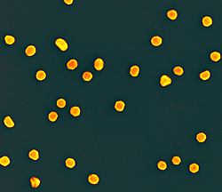 |
False color scanning electron micrograph (250,000 times magnification) showing the gold nanoparticles created by NIST and the National Cancer Institute’s Nanotechnology Characterization Laboratory (NCL) for use as reference standards in biomedical research laboratories.
Credit: Andras Vladar, NIST
View hi-resolution image |
The National Institute of Standards and Technology (NIST) has issued its first reference standards for nanoscale particles targeted for the biomedical research community—literally “gold standards” for labs studying the biological effects of nanoparticles. The three new materials, gold spheres nominally 10, 30 and 60 nanometers in diameter, were developed in cooperation with the National Cancer Institute’s Nanotechnology Characterization Laboratory (NCL).
Nanosized particles are the subject of a great deal of biological research, in part because of concerns that in addition to having unique physical properties due to their size, they also may have unique biological properties. On the negative side, nanoparticles may have special toxicity issues. On the positive side, they also are being studied as vehicles for targeted drug delivery that have the potential to revolutionize cancer treatments. Research in the field has suffered from a lack of reliable nanoscale measurement standards, both to ensure consistency of data from one lab to the next and to verify the performance of measurement instruments and analytic techniques.
The new NIST reference materials are citrate-stabilized nanosized gold particles in a colloidal suspension in water. They have been extensively analyzed by NIST scientists to assess particle size and size distribution by multiple techniques for dry-deposited, aerosol and liquid-borne forms of the material. Dimensions were measured using six independent methods—including atomic force microscopy (AFM), transmission electron microscopy (TEM), scanning electron microscopy (SEM), differential mobility analysis (DMA), dynamic light scattering (DLS), and small-angle X-ray scattering (SAXS). At the nanoscale in particular, different measurement techniques can and will produce different types of values for the same particles.
In addition to average size and size distributions, the new materials have been chemically analyzed for the concentrations of gold, chloride ion, sodium and citrate, as well as pH, electrical conductivity, and zeta potential (a measure of the stability of the colloidal solution). They have been sterilized with gamma radiation and tested for sterility and endotoxins. Details of the measurement procedures and data are included in a report of investigation accompanying each sample.
NCL examines candidate nanotech cancer drugs developed by biotech firms and academic labs. NCL and the NCI’s Alliance for Nanotechnology in Cancer sponsored the NIST work.
Additional technical and ordering information for the new NIST nanoparticle reference materials is available at:
Media Contact: Michael Baum, michael.baum@nist.gov, (301) 975-2763
NIST Develops Test Method for Key Micromechanical Property
Engineers and researchers designing and building new microelectromechanical systems (MEMS) can benefit from a new test method developed at the National Institute of Standards and Technology (NIST) to measure a key mechanical property of such systems: elasticity. The new method determines the “Young’s modulus” of thin films not only for MEMS devices but also for semiconductor devices in integrated circuits.
Since 1727, scientists and engineers have used Young’s modulus as a measure of the stiffness of a given material. Defined as the ratio of stress (such as the force per unit area pushing on both ends of a beam) to strain (the amount the beam is deflected), Young’s modulus allows the behavior of a material under load to be calculated. Young’s modulus predicts the length a wire will stretch under tension or the amount of compression that will buckle a thin film. A standard method to determine this important parameter—a necessity to ensure that measurements of Young’s modulus made at different locations are comparable—has eluded those who design, manufacture and test MEMS devices, particularly in the semiconductor industry.
A team at NIST recently led the effort to develop SEMI Standard MS4-1107, “Test Method for Young’s Modulus Measurements of Thin, Reflecting Films Based on the Frequency of Beams in Resonance.” The new standard applies to thin films (such as those found in MEMS materials) that can be imaged using an optical vibrometer or comparable instrument for non-contact measurements of surface motion. In particular, measurements are obtained from resonating beams—comprised of the thin film layer—that oscillate out-of-plane. The frequency at which the maximum amplitude (or velocity) of vibration is achieved is a resonance frequency, which is used to calculate the Young’s modulus of the thin film layer. The group also developed a special Web-based “MEMS calculator” (http://www.eeel.nist.gov/812/test-structures/MEMSCalculator.htm) that can be used to determine specific thin film properties from data taken with an optical interferometer.
Knowledge of the Young’s modulus values and the residual strain (using ASTM International Standard E 2245) for thin film layers can lead to calculations of residual stress, which in turn, enable semiconductor manufacturers to develop circuit design strategies, fabrication systems and post-processing methods that could increase fabrication yield by reducing the frequency of failures from electromigration, stress migration and delamination.
SEMI Standard MS4-1107 is available for purchase from SEMI, an international industry organization serving the advanced manufacturing community, at http://dom.semi.org/downloads.nsf/standard?openform&did=618EF551D3C0F6798825736300487EED&sid=0.
Media Contact: Michael E. Newman, michael.newman@nist.gov, (301) 975-3025
Quick Links
New Video Answers the Question 'What is NIST?'
For more than a century, the National Institute of Standards and Technology (NIST) has partnered with industry, academia and government to build an advanced science and technology infrastructure—the foundation needed to ensure continuing innovation, industrial competitiveness and the highest quality of life for all Americans. To help tell the story of how NIST affects your world daily, a new video feature, “What is NIST?”, has been posted and may be viewed by clicking here. You will need the latest Adobe Flash video player (download for free at http://www.adobe.com/products/flashplayer) to watch.
January Workshop to Focus on Safeguarding Health Care Information
The National Institute of Standards and Technology (NIST), in conjunction with the Centers for Medicare and Medicaid Services (CMS), is sponsoring a one-day workshop on security standards for safeguarding Electronic Protected Health Information (ePHI) as specified by the Health Insurance Portability and Accountability Act (HIPAA). As defined by HIPAA, ePHI is any protected health information that is created, stored, transmitted, or received electronically. The conference will focus on the HIPAA Security Rule, which specifies physical, technical, and administrative methods for protecting the electronic health information of individuals. It will be held on Jan. 16, 2008, at the NIST campus in Gaithersburg, Md.
The intended audience comprises professionals spanning both health care and information technology, including HIPAA rule implementers, privacy, compliance and security officers, and audit staff. Attendees will discuss challenges, tips, techniques and issues for implementing, adhering to and auditing the requirements of the HIPAA Security Rule.
The keynote speaker will be Anthony Trenkle, director of the CMS Office of E-Health Standards and Services. CMS is an agency of the U.S. Department of Health and Human Services. Attendees will also discuss the update to NIST Special Publication 800-66, An Introductory Resource Guide for Implementing the Health Insurance Portability and Accountability Act (HIPAA) Security Rule (http://csrc.nist.gov/publications/nistpubs/800-66/SP800-66.pdf).
Web registration for the workshop closes on Jan. 9, 2008, although attendees will be allowed to register by phone up until the time of the conference. For more information, go to http://www.nist.gov/public_affairs/confpage/080116.htm.
Workshop to Focus on Standards Education
Representatives of standards making bodies, corporate officials and educators from around the world will meet Feb. 21-22, 2008, at the “Global Perspectives and Strategies for Education about Standardization” workshop at the National Institute of Standards and Technology (NIST) in Gaithersburg, Md. Participants will discuss ways educate the next generation of business leaders on the importance of standards to commerce, technology commercialization and innovation. NIST will sponsor the meeting with ASTM International, the American National Standards Institute (ANSI) and its Committee on Education (CoE) and the International Committee for Education about Standardization (ICES).
The first day of the workshop will feature panel discussions of standards training in North America, South America and Asia. It will include reviews of current programs that integrate standards and conformity assessment into university curricula, along with examining the current state of standards professional training, continuing education and user training. On the second day, participants will identify key issues, needs and challenges facing those engaged in standards education, make suggestions for changes and discuss plans for future workshops to address them.
Workshop attendance is free; register at http://ts.nist.gov/Standards/ICES-Workshop.cfm. For more information, contact Erik Puskar, erik.puskar@nist.gov, (301) 975-8619.
|