| April 12, 2007

[NIST Tech Beat Search] [Credits] [NIST Tech Beat Archives] [Media Contacts] [Subscription Information]

Mass Weddings: NIST’s New Efficient 2-Photon Source
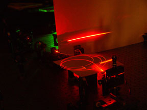 |
A microstructured optical fiber in NIST's new paired-photon source delivers high numbers of photon pairs over a broad bandwidth with low noise, all in a compact device for quantum communication devices.
Credit: Migdall/NIST
View hi-resolution image |
For a variety of applications in physics and technology, ranging from quantum information theory to telecommunications, it’s handy to have access to pairs of photons created simultaneously, with a chosen energy. In a significant improvement on previous designs, physicists at the National Institute of Standards and Technology (NIST) have devised a system that delivers such pairs with great efficiency over a wide range of energy, and with very little noise from extraneous photons*.
Paired photons can be generated—albeit very inefficiently—in standard optical media such as glass optical fibers. Photons normally travel through glass independently, without interacting, but if monochromatic laser light is sent down even an ordinary optical fiber, very occasionally two of the input photons will interact, producing an output photon pair with one higher in energy than the original photons and the other lower by the same amount.
Because the vast majority of photons go through the fiber unchanged, the relative intensity of these pairs is very small. Worse, the fiber generates the pairs randomly with a range of possible energies, so picking out those with some specific energy reduces the number of useful photon pairs still further. Worse yet, there is noise in the system due to the phenomenon called “Raman scattering,” in which individual photons bounce off the fiber’s molecular structure and change their energies. Scattering produces photons that look as if they might be one half of a pair, but aren’t.
To beat these odds, the new NIST two-photon source relies on a microstructured optical fiber. The fiber has a slender glass core at the center of an array of hollow channels, giving it a honeycomb appearance in cross-section. The geometrical structure of the fiber tightly restricts the way light can travel down it, increasing the intensity of light in the thin central core. Higher intensity means that photons are crowded more densely together, making events such as pair production more likely.
That greater efficiency allows the NIST researchers to get significant production of photon pairs by sending laser light through a mere 1.8 meters of the microstructured fiber, in contrast to the hundreds of meters of ordinary fiber that might be used in other systems. In addition, modifying the size of the channels in the microstructured fiber allows its properties to be optimized to reduce the amount of Raman scattering relative to the two-photon light of interest. The result is a source that produces significantly more pairs of photons over a wide frequency range, and with greatly reduced contamination by spurious Raman photons.
Photon pairs from the new source could be useful, for example, in exploring quantum “entanglement,” in which measurements on one of a pair of quantum particles with a common origin exert a subtle influence on the properties of the other, or in quantum cryptography.
*J. Fan and A. Migdall. A broadband high spectral brightness fiber-based two-photon source. Optics Express 15, 2915 (2007).
J. Fan, A. Migdall and L. Wang. A twin photon source based on optical fiber. Optics and Photonics News. March, 2007.
Media Contact: Michael Baum, michael.baum@nist.gov, (301) 975-2763 
Quantum Dot Lasers: One Dot Makes All the Difference
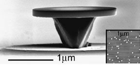 |
Microdisk lasers used in experiments by NIST, Stanford University and Northwestern University are made by layering indium arsenide on top of gallium arsenide and etching out disks about 1.8 micrometers across on pillars of gallium arsenide. Scanning tunneling microscope image (inset) shows some of the approximately 130 "quantum dot" islands of indium arsenide in each disk.
Credit: NIST
View hi-resolution image |
Physicists at the National Institute of Standards and Technology (NIST) and Stanford and Northwestern Universities have built micrometer-sized solid-state lasers in which a single quantum dot can play a dominant role in the device’s performance. Correctly tuned, these microlasers switch on at energies in the sub-microwatt range. These highly efficient optical devices could one day produce the ultimate low-power laser for telecommunications, optical computing and optical standards.
How small can a laser get? The typical laser has a vast number of emitters—electronic transitions in an extended crystal, for example—confined within an optical cavity. Light trapped and reflecting back and forth in the cavity triggers the cascade of coherent, laser light. But about a decade ago, researchers made the first quantum dot laser. Quantum dots are nanoscale regions in a crystal structure that can trap electrons and “holes,” the charge carriers that transport current in a semiconductor. When a trapped electron-hole pair recombines, light of a specific frequency is emitted. Quantum-dot lasers have attracted attention as possible embedded communications devices not only for their small size, but because they switch on with far less power then even the solid-state lasers used in DVD players.
In recent experiments*, the NIST-Stanford-Northwestern team made “microdisk” lasers by layering indium arsenide on top of gallium arsenide. The mismatch between the different-sized atomic lattices forms indium arsenide islands, about 25 nanometers across, that act as quantum dots. The physicists then etched out disks, 1.8 micrometers across and containing about 130 quantum dots, sitting atop gallium arsenide pillars.
The disks are sized to create a “whispering gallery” effect in which infrared light at about 900 nanometers circulates around the disk’s rim. That resonant region contains about 60 quantum dots, and can act as a laser. It can be stimulated by using light at a non-resonant frequency to trigger emission of light. But the quantum dots are not all identical. Variations from one dot to another mean that their emission frequencies are slightly different, and also change slightly with temperature as they expand or contract. At any one time, the researchers report, at most one quantum dot—and quite possibly none—has its characteristic frequency matching that of the optical resonance.
Nevertheless, as they varied a disk’s temperature from less than 10K to 50K, the researchers always observed laser emission, although they needed to supply different amounts of energy to turn it on. At all temperatures, they say, some quantum dots have frequencies close enough to the disk’s resonance that laser action will happen. But at certain temperatures, the frequency of a single dot coincided exactly with the disk’s resonance, and laser emission then needed only the smallest stimulation. It’s not quite a single-dot laser, but it’s a case where one quantum dot effectively runs the show.
*Z.G. Xie, S. Götzinger, W. Fang, H. Cao and G.S. Solomon. Influence of a single quantum dot state on the characteristics of a microdisk laser. Physical Review Letters, 98, 117401 (2007).
Media Contact: Michael Baum, michael.baum@nist.gov, (301) 975-2763
NIST’s Stretching Exercises Shed New Light on Nanotubes
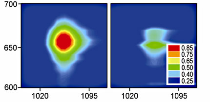 |
Biomedical applications could exploit the natural fluorescence of the carbon nanotubes. When light is polarized along a single-walled carbon nanotube (left), this fluorescent emission is strong. For perpendicular polarization (right), however, the emission disappears.
Credit: NIST
View hi-resolution image |
Stretching a carbon nanotube composite like taffy, researchers at the National Institute of Standards and Technology (NIST) and the Rochester Institute of Technology (RIT) have made some of the first measurements* of how single-walled carbon nanotubes (SWNTs) both scatter and absorb polarized light, a key optical and electronic property.
SWNTs have excited materials scientists with the promise of novel materials that have exceptional mechanical, electronic, and optical properties. One fundamental issue is how light interacts with SWNTs. Is there, for example, a way to use appropriately tailored light to exert a force on SWNTs so that they can be trapped or aligned? Or can they be designed to be nanoscale tags for medical diagnostics? Semiconducting SWNTs can fluoresce in the near infrared region, an ideal characteristic for medical applications because body fluids and tissues are nearly transparent in that range.
Recent research on the optics of SWNTs has focused on the behavior of “excitons” — the pairing of a negatively charged electron with the positively charged “hole” that it leaves behind when it gets excited by a photon into a higher energy state. An important optical characteristic is how excitons in SWNTs impact the way the nanotubes absorb and scatter light.For example, how easy is it for the incident light to deform an exciton to create positive and negative poles? Theory says it should be significantly harder to do in a nearly one-dimensional nanotube than in a bulk semiconductor, where nearby electrons and holes reduce the amount of energy required.
Measuring that is difficult because the effect depends on the orientation of the nanotubes, and they’re hard to line up neatly. The NIST/RIT team solved the problem elegantly by wrapping SWNTs with DNA to keep them from clumping together, and dispersing them in a polymer. When they heated the polymer and stretched it in one direction, the nanotubes aligned like sugar crystals lining up in pulled taffy, making the optical measurements possible. The team obtained the first experimental verification of the full optical response of individual semiconducting SWNTs, finding good agreement with theory.
The stretching alignment technique is applicable to a broad range of SWNT experiments where orientation is important, particularly in optics. The work should further our current understanding of how nanotubes interact with light, with important practical applications in optical sensing and the manipulation of individual nanotubes using electromagnetic fields.
* J.A. Fagan, J.R. Simpson, B.J. Landi, L.J. Richter, I.Mandelbaum, V. Bajpai, D.L. Ho, R. Raffaelle, A.R. Hight Walker, B.J. Bauer and E.K. Hobbie. Dielectric response of aligned semiconducting single-wall nanotubes. Physical Review Letters. 98, 147402 (2007).
Media Contact: Michael Baum, michael.baum@nist.gov, (301) 975-2763
NIST Releases Major Update of Popular REFPROP Database
The National Institute of Standards and Technology (NIST) has released an expanded and upgraded version of a popular database, a computer package for calculating the properties and modeling the behavior of fluids. Data on key components of alternative fuels, such as ethanol and hydrogen, are among the many new additions to NIST’s Reference Fluid Thermodynamic and Transport Properties Database Version 8.0, which provides critically evaluated property values needed to evaluate fluids and optimize related equipment and processes.
Widely used by industrial, academic, and government scientists, the database originally was called Refrigerant Properties and was limited to thermophysical properties of alternative refrigerants. When the previous version was issued in 2002, the name was changed to Reference Properties, denoting a broader range of fluids including some natural gas components. The latest version has been expanded further in response to user requests and NIST efforts to include more of the most widely used fluids.
Among its new features, Version 8.0 provides properties of ethanol, cryogenic fluids, and additional natural gas components. It also includes many new equations, which enable users to plug in variables such as temperature and pressure and find out how a fluid’s other properties, such as density and viscosity, stack up. In addition, many other aspects of the program have been enhanced, including the graphical interface.
NIST has distributed more than 4,000 copies of REFPROP since 1990. Thousands of additional copies are made available every year through commercial packages produced by companies that have distribution agreements with NIST. REFPROP has been the de facto standard in the refrigeration industry for years and is credited with helping industry find replacements for ozone-depleting chlorofluorocarbons (CFCs). Timely delivery of reliable data on the properties of alternative refrigerants made the search for CFC replacements more efficient, according to an economic impact study commissioned by NIST in the late 1990s.
More information about REFPROP, the NIST Reference Fluid Thermodynamic and Transport Properties Database (SRD 23), is available at www.nist.gov/srd/nist23.htm.
Media Contact: Laura Ost, laura.ost@nist.gov, (303) 497-4880
NIST Work Enhances Shop Floor Productivity
National Institute of Standards and Technology (NIST) engineers, together with colleagues from industry and other standards organizations have completed a five-part series of standards designed to evaluate the accuracy—and thus usability—of manufacturing measurements. The standards, the last of which was published last month by the American Society of Mechanical Engineers (ASME), describe ways measurement personnel can communicate, evaluate and respond to uncertainties in manufactured part measurements.
Adopting these standards on the shop floor should enhance manufacturing productivity at the same time that it minimizes scrapping of acceptable parts, unnecessary rework, and even litigation.
In a previous era, shop engineers could relax if component parts varied slightly from specification. Parts just had to “fit together.” However the complexity of many of today’s products, ranging from airplane turbines to nanotechnology microscopes, requires ever more advanced measurement capabilities at the shop floor. The ASME standards were needed because measurements often vary each time they are made (even the temperature of the part can change the measurement result by a significant amount). The series of standards also explains dimensional measurement traceability. Traceable measurements demonstrate the connection between the standard international (SI) unit of length (the meter) and the task-specific measurement under consideration; this also requires an uncertainty statement describing the accuracy of the measurement result.
The ASME B89.7 standards series addresses, with clear descriptions, the role of measurement uncertainty when accepting or rejecting products based on a measurement result and a product specification; economically efficient methods to overcome differences between two parties in the evaluation of measurement uncertainty; how to determine the economically appropriate decision to accept or to reject a product due to measurement uncertainty; and ways to demonstrate dimensional measurement traceability to the SI unit so that all parties can be sure of the reliability of their measurements. The latest addition to the series, B89.7.3.2, offers simplified guidelines for understanding and evaluating the major sources of measurement uncertainty.
NIST researchers chaired the ASME B 89.7 working groups and contributed to other related development work during the five-years it took to develop the five standards.
More information on the ASME B89 standards is available at: http://catalog.asme.org/home.cfm?SEARCH=B89.7.
Media Contact: John Blair, john.blair@nist.gov, (301) 975-4261
NIST/Industry Produce Improved Shock Tests
Extensive National Institute of Standards and Technology (NIST) work with industry, government, professional societies and standards developing organizations contributed to the release recently of an international standard for characterizing mechanical vibration and shock, and how systems from computer components to airframes and armored vehicles respond to specific kinds of shocks. The new standard published by the International Organization for Standardization (ISO) should be especially useful in environmental testing of products and components in high-technology industries such as computer and aerospace manufacturers.
NIST, as convener of the ISO working group that coordinated development of the standard, played an essential role in keeping United States industries informed of developments and encouraging U.S. industry participation in the international technical discussions to formulate the new standard.
The “shock response spectrum” (SRS) was developed originally as a method to describe the shock-like motions associated with earthquakes, explosions, impacts and other sources of mechanical shocks. An SRS shows graphically the relative strength of a shock pulse across a range of frequencies. For a mechanical system, such as an airframe, it can indicate how the system responds to a well-defined shock pulse. SRSs are used to describe both the severity of mechanical shocks and the ability of mechanical or electronic systems to tolerate them. They are widely used to test airframes and aerospace instrumentation systems, military vehicles and instrumentation systems used in them, mechanical isolation provided by shipping containers, the durability of hard drives, and to characterize explosive shock events. In the past, shock tests used a variety of analog and digital algorithms to synthesize SRS, which often produced significantly varying results. The new standard is based on standardized, well-defined digital techniques. It is a first step towards ensuring that the results of tests using an SRS can be compared reliably when performed at different laboratories.
ISO 18431-4:2007 “Mechanical vibration and shock—Signal processing—Part 4: Shock-response spectrum analysis” from the Acoustical Society of America, which sponsors the standards secretariat of the ISO Technical Committee responsible for this work, at http://asastore.aip.org/.
Media Contact: John Blair, john.blair@nist.gov, (301) 975-4261
Quick Links
Tips Can Help Consumers Choose Flat-Panel Displays
Choosing a flat-panel display for a television or video screen can be more complicated that you might think. Did you know, for instance, that the lighting in your living room can make a particular type of display look much better or worse than another?
Researchers at the National Institute of Standards and Technology (NIST) have worked with the private sector for years to develop measurement methods and standards for electronic displays used in industrial, medical, and consumer devices—diverse applications that require different approaches for evaluating performance. As part of this work, NIST developed the measurement technology required to characterize display properties such as contrast ratio, reflection, and color reproduction. Ed Kelley of NIST Optoelectronics Division in Boulder, Colo., has distilled his experience to a set of practical tips to help consumers know what to look for when evaluating different types of flat panel displays.
The tips can be found at www.fpdl.nist.gov/tips.html.
|