Stable Polymer Nanotubes
May Have a Biotech Future
Scientists
at the National Institute of Standards and Technology (NIST) have
created polymer nanotubes that are unusually long (about 1 centimeter)
as well as stable enough to maintain their shape indefinitely.
Described in a new paper in Proceedings of the National Academy
of Sciences,* the NIST nanotubes may have biotechnology applications
as channels for tiny volumes of chemicals in nanofluidic reactor
devices, for example, or as the “world’s smallest
hypodermic needles” for injecting molecules one at a time.
Carbon nanotubes are of keen interest in nanotechnology research,
especially for making ultrastrong fibers and other structures.
Nanotubes made from other materials are used for transport in
biochemical applications, but are typically fragile and usually
collapse within a few hours. The NIST team developed processes
for extending the shelf life of polymer nanotubes—considered
essential for commercial applications—and forming sturdy
nanotube network structures.
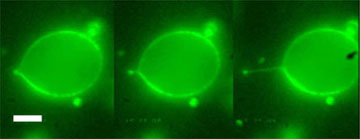
First the
researchers made tiny, fluid-filled spherical containers with
bi-layer membranes consisting of polymers with one end that likes
water and one end that does not. (These fluid-filled containers
are a spin-off of liposomes, artificial cells with fatty membranes
used in cosmetics and for drug delivery.) The researchers made
the membranes stretchy by adding a soap-like fluid to change the
polymer membranes’ mechanical properties. Then they used
“optical tweezers” (highly focused infrared lasers)
or tiny droppers called micropipettes to pull on the elastic membranes
to form long, double-walled tubes that are less than 100 nanometers
in diameter. (View
a movie of this process. (Requires Quicktime--download free).)
A chemical was added
to break bonds between atoms in one section of the polymers and
induce new bonds to form between the two different sections, forming
a rigid “cross-linked” membrane. The nanotubes are
then snipped free from the parent cell with an “optical
scalpel” (highly focused ultraviolet laser pulse). The nanotubes
maintain their shape even after several weeks of storage, and
can be removed from the liquid solution and placed on a dry surface
or in a different container. The optical tweezers can be used
to custom build nanotube network structures. The work was supported
in part by the Office of Naval Research.
*J.E. Reiner,
J.M. Wells, R.B. Kishore, C. Pfefferkorn, and K. Helmerson. 2006.
Stable and robust polymer nanotubes stretched from polymersomes.
Proceedings of the National Academy of Sciences. Published
online Jan. 23, 2006.

NIST
Issues Final Federal Biometric Specs
The
National Institute of Standards and Technology (NIST) yesterday
issued the final publication describing how biometrics should
be stored on Personal Identity Verification (PIV) cards. These
cards will be required for all federal employees and contractors
beginning in October 2006.
NIST Special
Publication 800-76, Biometric Data Specification for Personal
Identity Verification, contains specifications for acquiring,
formatting, and storing fingerprint images and templates; for
collecting and formatting facial images; and specifications for
biometric devices used to collect and read fingerprint images.
The publication specifies that two fingerprints be stored on the
card as “minutia templates,” mathematical representations
of fingerprint images.
In August
2004, the President issued Homeland Security Presidential Directive
12 calling for a mandatory, government-wide personal identification
card that all federal government departments and agencies will
issue to their employees and contractors requiring access to federal
facilities and systems.
Federal Information
Processing Standard 201, Personal Identity Verification for Federal
Employees and Contractors, approved by Commerce Secretary Carlos
Gutierrez on Feb. 25, 2005, specifies the technical and operational
requirements for the PIV system and cards. NIST Special Publication
800-76 is a companion document to FIPS 201 describing how the
standard will be implemented.
For a copy
of SP 800-76 and more information on PIV, see http://csrc.nist.gov/piv-program/index.html.
Fire Panel Changes Offer Real-Time Fire Status
Data
Fire
panels, or “annunciators,” are electronic devices
that display data on building conditions in one easily accessible
location. When used by first responders during emergencies,
the devices can save lives. In December 2005, the National
Electrical Manufacturing Association (NEMA) released a comprehensive
standard* that promises to make future annunciators even
more useful decision-making tools to fire fighters at the
scene, to commanders back at headquarters, or to building
and emergency personnel rushing to a fire.
Developed
with the help of the National Institute of Standards and
Technology (NIST) and the U.S. fire alarm industry, the
standard offers greater uniformity in design, operation
and arrangement of fire panels, common symbols denoting
fire-related building conditions, and equipment specifications
concerning wireless and remote applications. The standardization
effort should make real-time information of value clearly
and quickly available for processing, planning and response.
For instance, agreement on how to unambiguously represent
conditions such as biochemical hazards or the locations
of smoke vents and elevators should make the fire panels
and related equipment much better tools for rapid decision-making.
Similar display and message symbols also should save time
and training funds currently needed to teach fire fighters
to understand dissimilar fire panel systems. Finally, standardization
is considered necessary for parallel efforts in the first
responder community to develop a capability to transmit
relevant, easy-to-understand building and fire emergency
information to fire fighters prior to their arrival on the
scene.
In
a related development, NIST released proceedings of a July
26, 2005, workshop** held at its Gaithersburg, Md., campus
in which fire safety personnel used laptops to simulate
and to evaluate the usefulness of transmitting real-time
fire panel data to dispatch centers and to officers at the
scene monitoring fire fighters during an emergency. Participants
considered four scenarios: (1) a hospital fire; (2) arson
in a third-floor laboratory building room; (3) fire on the
second floor of a two-story single family dwelling; and
(4) an emergency medical call inside a large shopping mall.
The final report lists almost 100 recommendations for improvements
of current displays, ranging from suggestions for different
colors for various fire conditions, better depiction of
evacuation stairwell size, and even off-site screen printout
capability.
*A
copy of the NEMA annunciator standard, SB 30-2005 (Fire
Service Annunciator and Interface), is available for purchase
at http://www.nema.org/stds/sb30.cfm.
**NIST’s
Workshop on the Evaluation of a Tactical Decision Aid
Display (NISTIR 7268) is available at http://fire.nist.gov/bfrlpubs/fire05/PDF/f05105.pdf (.pdf;
download Acrobat Reader).
The Department of Justice Community Oriented Policing Service
(COPS) sponsored the workshop via the NIST Office of Law
Enforcement Standards (OLES).
Media
Contact:
John
Blair, john.blair@nist.gov,
(301) 975-4261
New
Design for Transistors Powered by Single Electrons
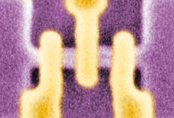 |
Colorized
micrograph of three tunable gates across an electrical channel
in a single electron tunneling (SET) transistor.
Credit:
NTT/NIST
View
high resolution of this image. |
Scientists
have demonstrated the first reproducible, controllable silicon
transistors that are turned on and off by the motion of individual
electrons. The experimental devices, designed and fabricated at
NTT Corp. of Japan and tested at NIST, may have applications in
low-power nanoelectronics, particularly as next-generation integrated
circuits for logic operations (as opposed to simpler memory tasks).
The transistors,
described in the Jan. 30, 2006, issue of Applied Physics Letters,*
are based on the principle that as device sizes shrink to the
nanometer range, the amount of energy required to move a single
electron increases significantly. This makes it possible to control
individual electron motion and current flow by manipulating the
voltage applied to barriers, or "gates," in the electrical
circuit. At negative voltage, the transistor is off; at higher
voltage, the transistor is turned on and individual electrons
file through the circuit, as opposed to thousands at a time in
a conventional device.
This type
of innovative transistor, called a "single-electron tunneling"
(SET) device, is typically made with a metal “wire”
interrupted by insulating barriers that offer a rigid, narrow
range of control over electron flow. Silicon devices, by contrast,
have barriers that are electrically "tunable" over a
wider operating range, offering finer, more flexible control of
the transistor’s on/off switch. Particular voltage levels
are applied across the barriers, to manipulate charge, as a means
of encouraging or impeding electron flow. Silicon-based devices
also allow fabrication using standard semiconductor technology.
Until now, however, no silicon SET transistor designs have been
reported that are reproducible and controllable.
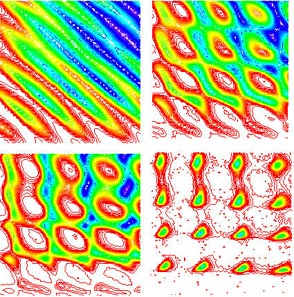 |
The
colorized images show how tuning the voltage of the three
gates controls very small amounts of electrical charge and
regulates current flow in the new silicon transistor. In
the first figure, the pattern of diagonal lines indicates
the charge is correlated throughout the device, and current
is flowing (at levels ranging from 0 Amps shown in red,
to 1.4 nanoAmps shown in violet). The next three figures
show what happens as the voltage applied to the center gate
is reduced. In the last figure, the square pattern indicates
the charge has separated in the device, and the large amount
of white space indicates a related drop off in the current.
Credit:
NTT/NIST
View
high resolution of this image.
|
The NIST/NTT
team made five uniform, working silicon transistors with tunable
barriers. Each device consists of a silicon channel 360 nanometers
(nm) long and 30 nm wide, with three gates crossing the channel.
The gates have two levels; the upper level turns the current on
and off, while the lower level controls electron flow in small
local areas. The team was able to tune gate conductance properties
over a wide range, by more than three orders of magnitude.
This work was partly supported by the Japan Society for the Promotion
of Science.
*A. Fujiwara,
H. Inokawa, K. Yamazaki, H. Namatsu, Y. Takahashi, N.M. Zimmerman,
and S.B. Martin. 2006. Single electron tunneling transistor with
tunable barriers using silicon nanowire MOSFET. Applied Physics
Letters. Jan. 30.
Media
Contact:
Laura
Ost, laura.ost@nist.gov,
(301) 975-4034

Enhanced
LIDAR Improves Range, Vibration Measures
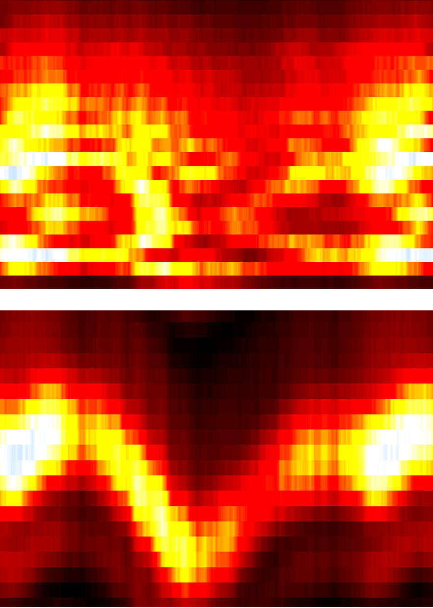
 |
Conventional
laser ranging systems would fail to produce usable data
on the range to a target about 1 kilometer away (false color
image, top). By contrast, the NIST system obtains a clear
image of the relative changes in the range to the target
with time. The rise and fall of the plot (bottom) represents
very small changes in range from the detector to the surface
of a rotating, wobbling disk.
Credit:
NIST/N. Newbury, W. Swann
View
high resolution of this image.
|
Scientists
at the National Institute of Standards and Technology (NIST) have
demonstrated the use of an ultrafast laser “frequency comb”
system for improved remote measurements of distance and vibration.
The technology, described in a forthcoming issue of Optics
Letters,* may have applications in automated manufacturing
or defense systems because it enables unusually precise characterization
of the range profile and motion of a surface.
The NIST
laboratory system is an adaptation of light detection and ranging
(LIDAR), which transmits light through the air to a target and
analyzes the weak reflected signal to measure the distance, or
range, to the target and other parameters. The NIST system uses
an infrared laser that emits a continuous train of very brief,
closely spaced pulses of light of many colors, or frequencies.
An analysis of the frequencies reveals a very fine “comb”
of evenly spaced teeth. The short pulse length (quadrillionths
of a second, or millionths of a billionth of a second) creates
a wide range of comb frequencies, enabling more accurate range
measurements; the inherent stability of the laser creates fine
comb teeth, enabling very precise vibration measurements.
The frequency
comb serves as both the light source and as a precise ruler for
measuring the reflected signal. NIST-developed software analyzes
the intensity of the reflected signal to measure distance to the
target, and analyzes the frequency (or Doppler) shift to measure
vibration. The most unusual aspect of the system is the way it
resolves common problems with signal “noise” and dispersion
of light by the atmosphere into longer pulses (with different
colors of light traveling at different speeds). The reflected
light that is detected is divided into a number of different color
bands for computer processing. Measurements are averaged across
the channels, effectively multiplying the precision of the result
by the number of channels.
The system
was used to determine the distance to, and vibration of, a rotating
disk located on the far side of the laboratory. Experiments were
conducted under a variety of conditions. For example, with the
reflected light transmitted over an extended distance (partly
through 1 kilometer of optical fiber wrapped around a spool),
the NIST system could measure a 45-micrometer displacement across
the disk surface at a range of 1 km thanks to the signal processing
method. Conventional LIDAR would have failed at that distance
due to dispersion of the reflected light within the fiber, according
to the paper.
* W.C. Swann
and N.R. Newbury. 2006. Frequency-resolved coherent LIDAR using
a femtosecond fiber laser. Optics Letters. Scheduled
for the March 15 issue. Posted online Nov. 23, 2005.
Media
Contact:
Laura Ost, laura.ost@nist.gov,
(301) 975-4034
