| July
13, 2005

[NIST
Tech Beat Search] [Credits] [NIST Tech Beat
Archives] [Media
Contacts] [Subscription Information]

JILA
Study of RNA Dynamics May Help in Drug Design
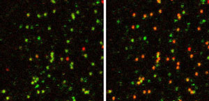 |
These false-color images show the behavior of about 30
to 40 single RNA molecules tagged with fluorescent
dyes in the absence of magnesium (left) and with
high magnesium concentrations (right). Green indicates
that the tagged molecules are farther apart (undocked)
whereas red indicates they are closer together (docked),
showing that magnesium promotes docking.
Click
here for a high-resolution version of this image.
|
Biophysicists
have developed a method for studying, in real time, a nanoscale “docking
and undocking” interaction
between small pieces of ribonucleic acid (RNA), a technique
that may be broadly useful in studying structural changes
in RNA that affect its function. The research at JILA, a
joint institute of the National Institute of Standards and
Technology (NIST) and University of Colorado at Boulder,
may have applications in the design of effective new drugs
based on small RNA strands.
RNA is
a chain-like molecule that contains genetic information,
makes
proteins and catalyzes biological reactions. Scientists at
JILA are studying RNA using methods that reveal how individual
chemical units of RNA dock, or lightly and temporarily bond,
to form special three-dimensional shapes that exhibit biochemical
activity. The latest work, to be published the week of July
11 in the Proceedings of the National Academy of Sciences,*
adds to understanding of the intramolecular “stickiness”
between specific loops and sequences in the RNA that help stabilize
this folding. This type of information is crucial to understanding
RNA structure and, ultimately, how it affects function.
The JILA
group developed a simple model system for studying the reversible
docking of a small piece of RNA at a receptor
site in the same molecule. They used a technique called fluorescence
resonance energy transfer, in which the two pieces of RNA are
labeled with different dyes that have overlapping emission
bands. One dye emits light of the same color that the other
dye absorbs; the second dye then emits light of a different
color. One piece of RNA is excited by a laser and, when the
two pieces are close enough together to dock, passes energy
to the other one, which then fluoresces. This method was used
to measure the distance between the two pieces of RNA as it
varied from less than 4 nanometers in the docked state to about
7 nm in the undocked state.
The scientists
used ultrasensitive laser-based microscopy methods to image
many isolated RNA molecules simultaneously, in effect generating
a “movie” of single molecule docking kinetics in
real time. They used this method to study thousands of pieces
of RNA over time scales of 10 to 30 seconds, and observed about
two-thirds of them rapidly docking and undocking. The rates
of docking and undocking were measured as a function of the
concentration of magnesium ions in the surrounding fluid, revealing
a complex dependence on metal ions, as is typical for RNA. The
docking rate rose 12-fold as magnesium concentrations increased.
A significant number of molecules still docked in the absence
of magnesium—the first time this phenomenon has been observed,
according to the paper.
The research
is supported by NIST, the National Science Foundation, National
Institutes of Health, and the W.M. Keck Foundation
initiative in RNA science at CU-Boulder.
*J.H. Hodak,
C.D. Downey, J.L. Fiore, A. Pardi and D.J. Nesbitt 2005. Docking
kinetics and equilibrium of a GAAA tetraloop-receptor motif
probed by single molecule fluorescence resonance energy transfer.
Proceedings of the National Academy of Sciences. Week
of July 11.
Temperature
Control Improves NIST X-ray Detector
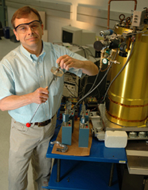 |
| Research
physicist Terrence Jach prepares to analyze a sample
with the NIST X-ray microcalorimeter. Improved temperature
sensing and control systems allow the instrument within
the gold chamber to the right to detect X-rays characteristic
of specific elements over a broad range of energies
with higher resolution.
Photo
credit: Gail Porter/NIST
Click
here for a high-resolution version of this image.
|
Researchers
at the National Institute of Standards and Technology (NIST)
have developed an improved experimental X-ray detector that
could pave the way to a new generation of wide-range, high-resolution
trace chemical analysis instruments. In a recently published
technical paper*, the researchers described how they used
improved temperature-sensing and control systems to detect
X-rays across a very broad range of energies (6 keV or more),
with pinpoint energy resolution (an uncertainty of only 2
eV).
The
detector’s ability to distinguish
between X-rays with very similar energies should be especially
useful to
the semiconductor industry for chemical analysis of microscopic
circuit features or contaminants. Many types of high-resolution
microscopes routinely used in the industry and throughout
science produce detailed chemical maps by scanning a surface
with electrons and then analyzing the X-rays emitted, which
are characteristic of specific elements.
The
NIST device, an improved version of its previous microcalorimeter
X-ray
detector, uses a quantum-level, transition edge sensor
(TES). NIST has led development of these sensors for
several years. A TES works by measuring the current across
a thin
metal film that is held just at the knife-edge transition
temperature between a superconducting state and normal
conductance. A single X-ray photon striking the detector
raises the temperature
enough to alter the current proportional to the energy
of the photon.
TES
microcalorimeters offer an unequaled combination of high
resolution with detection of a broad
energy range,
allowing
identification of many different chemical elements
simultaneously. The two kinds of detectors conventionally
used in X-ray
microanalysis typically have a resolution of no better
than 130 eV, or
have a high resolution but only for a very narrow range
of energies. TES sensors, however, must be kept at
very low
temperatures (about 97 millikelvin) for hours at a
stretch to collect trace-level data. Tiny changes in temperature
would cause previous versions of the instrument to “drift” over
time, requiring constant recalibrations. The improved
temperature control system for the new detector eliminates
this problem,
making the system much more practical for a broad range
of applications.
*T.
Jach, J.A. Small and D.E. Newbury. Improving energy
stability in the National Institute of Standards and Technology
microcalorimeter
X-ray detector. Powder Diffraction v. 20,
No. 2, June 2005.
Media
Contact:
Michael
Baum, michael.baum@nist.gov, (301) 975-2763
New
Infrared Tool Measures Silicon Wafer Thickness
 |
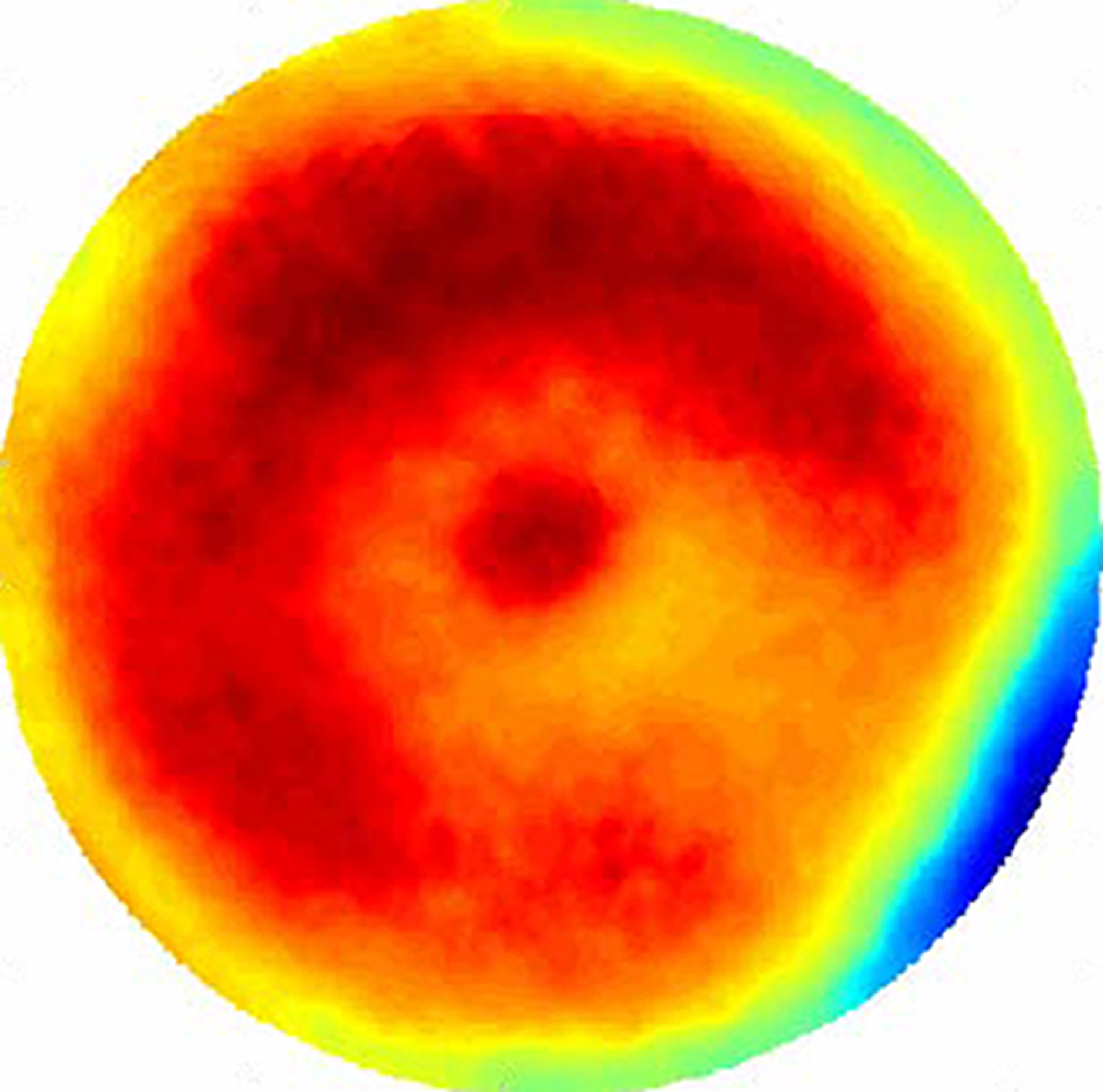
A new NIST calibration system under development used
infrared laser light to precisely measure the
thickness of 300
millimeter silicon wafers. Changes in color within the
spatial map above represent changes in wafer thickness.
Green represents the average wafer thickness, while red,
orange and yellow areas are thicker, and turquoise
and
blue areas are thinner.
Credit:
Q. Wang, U. Griesmann/NIST
Click
here for a high-resolution version of this image.
|
In
the last few years, semiconductor circuit features have shrunk
to sub-100 nanometer (nm) dimensions, while the size of the
thin silicon wafers that these circuits are constructed on
has grown from 200 millimeters (mm) to 300 mm (about 12
inches). The payoff is a higher yield of finished devices
from fewer wafers.
The tough
part, however, is to make wafers substantially larger while
simultaneously meeting higher
quality control
specifications.
The optics and materials for “printing” nanoscale
circuit lines require that the wafers used are perfectly
flat and of uniform thickness. To help the semiconductor
industry
meet its 2010 quality control roadmap goals, researchers
at the National Institute of Standards and Technology (NIST)
recently
developed a new instrument that accurately measures differences
in thickness across a 300 mm wafer with an excellent repeatability
of 5 nm. The researchers hope the tool, with further refinements,
will allow them to establish a new calibration service for “master
wafers” used in the industry to measure wafer thickness.
The NIST
researchers will describe the instrument, the Improved Infrared
Interferometer, or IR3 for short, at a technical
conference* in late July. Like all interferometers, the IR3
uses intersecting waves of light to create interference patterns,
which in turn can be used as a ruler to measure nanoscale dimensions.
While most interferometers use red laser light, the IR3
uses infrared laser light. And unlike visible light, these much
longer wavelengths pass right through a silicon wafer. This
means that IR3 can illuminate the top and bottom
on a 300 mm wafer and produce a detailed spatial map of differences
in thickness in one pass. Conventional tools require spinning
the wafer and measuring at multiple locations.
The NIST
researchers make precision measurements of the wafer’s
index of refraction—the amount that light is “bent” as
it passes through the silicon—as a critical step
in correctly interpreting the interference patterns.
Increased precision
in the refractive index measurement will be necessary
before “absolute” measurements
of thickness rather than relative differences will be
possible with the new instrument.
*Q. Wang,
U. Griesmann and R. Polvani. Interferometric thickness
calibration of 300 mm silicon wafers. ASPE Summer Topical
Meeting on Precision Interferometric Metrology (July 20-22,
2005).
NIST
Finds Rough Spot in Surface Measurement
For makers of computers, disk drives and
other sophisticated technologies, a guiding principle is the
smoother the surfaces of chips and other components, the better
these devices and the products, themselves, will function.
So, some manufacturers might be surprised
to learn that a fast and increasingly popular method for measuring
surface texture can yield misleading results. As reported
at recent conferences and in an upcoming issue of Applied
Optics,* a team of National Institute of Standards and
Technology researchers has found that roughness measurements
made with white light interferometric microscopes, introduced
in the early 1990s, differed by as much as 80 percent from
those obtained with two other surface-profiling methods.
Interferometric microscopes are used to measure
surface heights, lengths and spaces by analyzing the interference
patterns created by two light beams—one reflected by
a reference specimen and the other by the object of interest.
To date, the team has evaluated a total of
five white light instruments from three different vendors.
They compared roughness measurements of gratings with both
wavelike surfaces and random surfaces.
White light interferometers were compared
with “phase shifting" interferometers, which use
specialized single-color light sources, and with accurate,
but sometimes destructive, stylus profiling instruments that
trace a sharp probe over a surface. The latter two tools were
in agreement across the spectrum of test samples within the
expected measurement range of the phase shift interferometers.
For measurements of relatively rough surfaces, white light
interferometers also yielded results that corresponded closely.
But for measurements of surfaces with an average roughness
between 50 and 300 nanometers, results diverged significantly,
peaking at about 100 nanometers.
“The discrepancy seems to be unrelated
to the specific white light instrument used or to the randomness
of the surface profile,” explains Ted Vorburger, head
of NIST’s Surface and Microform Metrology Group.
The comparative study was carried out as
part of an effort to develop international standards for three-dimensional
measurements of surface texture. NIST researchers are now
evaluating theoretical explanations for the observed discrepancies.
H.G. Rhee, T.V. Vorburger, J.W. Lee and
J. Fu, Discrepancies between roughness measurements obtained
with phase shifting interferometry and white-light interferometry.
Applied Optics, 2005.
Media Contact: Mark Bello, mark.bello@nist.gov,
(301) 975-3776
Predicting
the Lifetime of Extreme UV Optics
Extreme
ultraviolet lithography (EUVL) may be the next-generation
patterning technique used to produce smaller and faster
microchips with feature sizes of 32 nanometers and below.
However, durable projection optics must be developed before
this laboratory technique can become commercially viable.
As part of its long-standing effort to develop EUVL metrology
and calibration services (summarized in a recent paper*),
the National Institute of Standards and Technology (NIST)
is creating a measurement system for accelerated lifetime
testing of the mirrors used in EUVL.
The
light to be used in EUVL has a wavelength of only 13 nm.
It can only be
efficiently reflected with mirrors consisting
of 50 alternating bi-layers of molybdenum and silicon, each
only 7 nm thick and deposited with near-atomic-scale precision.
So although the EUVL mirrors
will be very large, up to 35 centimeter (cm) in diameter,
they are actually incredibly precise nanostructured devices.
A single commercial lithography instrument may require
six of these mirrors at a cost of more
than $1 million each.
The
mirrors are delicate, but the EUV radiation they must reflect
is intense and damaging. The
combination of this
harsh radiation
with the trace levels of water vapor and hydrocarbons typically
found in the vacuum environment of EUV first-generation
exposure tools can lead to rapid corruption of the EUVL
mirror surfaces.
And a loss of just 1 percent to 2 percent of a mirror’s
reflectivity renders the optical system useless for efficient
production
of nanometer-resolution circuit features.
To
help the semiconductor industry meet its goal of EUVL production
by 2010, NIST
has established a dedicated beamline
at its Synchrotron Ultraviolet Radiation Facility for durability
testing of multilayer mirrors.
Initial tests established that standard mirrors topped
with silicon
would have lifetimes of just minutes to hours, while
ruthenium-capped mirrors had lifetimes of a few tens of
hours, still a thousand
times less than industry’s requirement.
To
determine how damage scales with various parameters, NIST
researchers
recently exposed EUVL mirrors (provided
by SEMATECH
from work it co-funded) to varying levels of light intensity,
water and hydrocarbon concentrations.
Contrary
to expectations, they found that increasing amounts of water
vapor caused less mirror damage, which may be due to a simultaneous
increase in the ambient hydrocarbon levels. Subsequent experiments
have shown that deliberately introducing trace amounts of a
simple hydrocarbon like methanol can mitigate significantly
the water-induced damage. NIST scientists are commissioning
a new beamline devoted to accelerated testing and will add a
second branch to the existing beamline that will provide broadband
illumination (wavelengths of approximately 11 nm to 50 nm) into
a single spot at approximately 100 times the intensity of the
current system.
For further
information, see http://physics.nist.gov/euvl.
*S.
Grantham, S.B. Hill, C. Tarrio, R.E. Vest and T.B. Lucatorto.2005.
EUV component and system characterization at NIST for the support
of extreme-ultraviolet lithography. Proceedings of SPIE
5751, 1185-91.
Media
Contact:
Laura
Ost, laura.ost@nist.gov, (301) 975-4034
|

