| Nano at NIST:
Recent Nanotechnology Accomplishments
Researchers at the National Institute of Standards and Technology (NIST) are developing measurements, standards, and data crucial to private industry’s development of products for a global nanotechnology market that could top $2 trillion during the next decade. NIST researchers are also helping other federal agencies to exploit nanotechnology to further their missions in areas including national security, food safety, and environmental protection.
Nanotechnology components were incorporated into almost $90 billion worth of manufactured products in 2001, an increase of about 75 percent over the previous year. Still to come are ever-more capable, high-value-added products that will exploit growing knowledge of the extraordinary properties and behaviors of materials at the nanoscale, defined as 1 nanometer (equivalent to a row of 10 hydrogen atoms) to 100 nanometers (about a thousandth of the diameter of a fine human hair). Ultimately, this accelerating revolution in nanotechnology will set the future course of industries and economies around the globe.
The NIST laboratories are helping to develop the nation’s technical infrastructure for nanotechnology, often in partnership with U.S. companies and other organizations, all the way from lab to market. The advanced tools resulting from these efforts are necessary to ensure that the United States will reap the full economic and social benefit from the billions of public and private dollars invested in nanotechnology research.
Through its Technology Innovation Program (TIP), NIST also provides funding to support nanotechnology advances targeted to critical national needs. In addition, the NIST-managed Hollings Manufacturing Extension Partnership provides technical services that help the nation’s smaller manufacturers apply best practices and develop the capabilities needed to capitalize on nanotechnology-enabled opportunities.
NIST is a key contributor to the National Nanotechnology Initiative, the 26-agency federal effort to speed progress in nanoscale science, engineering, and technology. In 2008, more than 150 nanotechnology research projects were under way at NIST. A sampling of recent accomplishments and milestones follows.
1Matthew Nordan, Lux Research, “Testimony before the Senate Committee on Commerce, Science, and Transportation,” April 24, 2008.
Facilities & Partnerships
Nanofab Provides Access
to Cutting-Edge Equipment
NIST’s new Center for Nanoscale Science and Technology (CNST) recently began accepting proposals for work in its Nanofab, a user facility for nanotechnology research. The CNST offers researchers from universities, industry, and other government agencies access to state-of-the-art and beyond-state-of-the-art facilities to study a wide range of nanotechnology topics.
The new center focuses on overcoming major technical obstacles to cost-effective manufacturing of products made with components the size of atoms and molecules. It develops measurement methods, standards, and technology that help emerging nanotechnologies move from the laboratory to production.
The CNST Nanofab is located within NIST’s Advanced Measurement Laboratory, one of the most advanced research facilities of its kind in the world. The building includes a 19,000-square-foot bay-and-chase cleanroom, with 8,000 square feet of class 100 space, 1,000 square feet of class 1,000 lab space, and 10,000 square feet of class 1,000 support space.
The NanoFab features more than 30 state-of-the-art tools such as photolithography and ion beam and etching equipment capable of creating, measuring, and inspecting nanoscale devices with dimensions as small as 10 nanometers.
Researchers interested in working at the facility can submit proposals for review in any nanotechnology research area. CNST will accept both proprietary and non-proprietary research proposals. Non-proprietary research may qualify for a partial waiver of user fees if the project falls within CNST’s mission. Non-proprietary proposals are expected to lead to publication of research results in the open scientific literature.
Detailed information about the proposal process, available facilities, current CNST research programs, and contact information for fee schedules is available at cnst.nist.gov.
NIST, SRC-NRI Partnership Drives Search for Next-Generation Computer Technology
NIST and the Semiconductor Research Corporation (SRC) recently entered a public-private partnership to support research and innovation in nanoelectronics, an emerging area in electronics that exploits the unique properties of nanometer-scale materials. The partnership will fund a variety of high-priority research projects identified by the Nanoelectronics Research Initiative (NRI), which coordinates research in nanoelectronics among major universities across the country. The goal is to develop practical future-generation successors to today’s computer technology. NIST has contributed $2.76 million to the effort thus far, with additional funds from SRC’s industry partners. In April, the partnership announced an additional $11.2 million of nanoelectronics funding for the next three years, for a total of
$15 million.
One of the new awards established a new nanoelectronics research center on the campus of the University of Notre Dame. Receiving a total of $61 million in funding from the NRI, major chip manufacturers and the state of Indiana, the new Midwest Academy for Nanoelectronics and Architectures will link five universities with the development resources of national laboratories and the trillion-dollar per year technology industry. Collaborators will work to develop and exploit a new class of semiconductor materials and devices that stretches beyond today’s state-of-the-art chip
technologies.
Research at the Notre Dame-based center is expected to commence later in 2008.
Other awards went to the three pre-existing nanoelectronics centers located on university campuses in California, Texas, and New York. The awards will support the investigation of broad research topics at each center and fund individual projects. Over two dozen universities from all across the United States now belong to the four centers, and the list is growing. Each center is aimed at furthering the development of nano-sized electronic devices, and all have become the seed for expanded technology investment and economic development for local communities.
After an open competition held in May 2007, NIST chose NRI as an industry-led consortium with which NIST could partner to accelerate research in electronics that goes beyond today’s building-block technology, referred to as CMOS.
“Our teaming with the Nanoelectronics Research Initiative is part of a NIST-wide effort to explore new models of public-private partnerships to accelerate and promote innovation,” said NIST Chief Scientist Richard Kayser. “We look forward to the challenging work ahead to take nanoelectronics and the U.S. economy to new levels of accomplishment, competitiveness, and growth.”
NIST Signs Cooperative Agreement with U-Albany Nano College
NIST and the College of Nanoscale Science and Engineering (CNSE) of the University at Albany-State University of New York have initiated cooperative efforts to develop science and technology for measuring materials at the nanometer scale as well as creating new standards for nanomanufacturing.
Leaders of the two organizations signed a memorandum of understanding (MOU) on April 21, 2008, at a ceremony hosted by Senator Charles E. Schumer (D-N.Y.) at CNSE’s Albany NanoTech Complex, which houses more than 2,000 employees, including many from the semiconductor industry.
NIST and CNSE will establish policies and general procedures for cooperating and coordinating efforts in areas of common interest. Developing state-of-the-art nanoscale measurement tools and standards is necessary for creating ever-smaller computer chips that perform tasks more quickly and reduce power consumption for a wide range of electronic devices from cell phones to desktop computers.
“Our shared aim is to develop the measurement science infrastructure that is absolutely essential to U.S. innovation and economic competitiveness in nanotechnology,” said NIST Deputy Director James M. Turner. “NIST is eager to forge a productive collaboration that leverages this impressive collection of intellectual and physical resources.”
The MOU follows the creation earlier this year of the New York Center for National Competitiveness in Nanoscale Characterization (NC3) at CNSE. Funding for the center was provided under NIST’s FY 2008 appropriation. By working to advance innovations in nanoscale measurement science, NC3 strives to strengthen the relationships between nanotech R&D, manufacturing, and commercialization.
Processing, Fabricating, Manufacturing
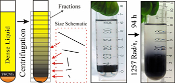 |
In a schematic of NIST's length separation technique for carbon nanotubes (l.), the nanotubes start at the bottom of a dense fluid. When spun in a centrifuge, the nanotubes begin to migrate through the fluid driven by their buoyancy, but the longer ones move faster, spreading them out by length. Photos (r.) shows a typical sample at the start and after 94 hours of spinning at 1,257 radians per second (roughly 12,000 RPM).
Credit: NIST
View hi-resolution image |
Spin Control: New Technique
Sorts Nanotubes by Length
A new technique to sort batches of carbon nanotubes by length using high-speed centrifuges has been reported by NIST researchers.* Many potential applications for carbon nanotubes depend on the lengths of these microscopic cylinders. The new technique should be easily scalable to produce industrial quantities of high-quality nanotubes, the scientists say.
So-called single-wall carbon nanotubes (SWCNTs) are essentially rolled sheets of carbon atoms, one atom thick and about a nanometer in diameter. They have unique combinations of thermal, mechanical, optical, and electronic properties that suggest a wide variety of uses, including circuit elements in molecular electronics,
fluorescent tags for diagnostic and therapeutic applications in medicine, and light sources for compact, efficient flat-panel displays.
Unfortunately, the methods for manufacturing carbon nanotubes always create a large percentage of nanojunk in the mix—clumps of carbon, ordinary soot, particles of metal used as a catalyst—and nanotubes come in an enormous range of lengths, from a few tens or hundreds, up to thousands of nanometers. Refining the lot is essential for most uses. For many potential applications, nanotubes need to be separated by length. In biomedical applications, for example, it has been shown that whether or not nanotubes are taken up in cells depends critically on length. Nanotube components in future microcircuits obviously will need to fit in place. In
optical applications, nanotube lengths determine how strongly light will be absorbed or emitted.
In 2006, researchers found that you could separate nanotubes by “chirality” (a measure of the twist in the carbon atom sheet) by spinning them in a dense fluid in an ultracentrifuge tube because of a relationship between chirality and buoyancy. In this new work, a NIST team demonstrated that a variation of the same technique can separate nanotubes by length. They showed that while the nanotubes ultimately will move to a point of equilibrium in the centrifuge tube dictated by their buoyancy, due to friction they will move at different rates depending on their lengths.
“When we spin the centrifuge, it turns out that the longer ones move faster. We basically just run a race and the longer ones move farther in the same amount of time,” says researcher Jeffrey Fagan. “Eventually they get separated enough in position that we can just pull off layers and get different lengths.”
What’s particularly exciting, they say, is that while other techniques have been shown to sort nanotubes by length, this is the first approach that could be scaled up to produce commercially important quantities of nanotubes in a given length range. The process also removes much unwanted junk—particularly metal particles—from the batch. NIST has applied for a patent on the process.
*J.A. Fagan, M.L. Becker, J. Chun, and E.K. Hobbie. Length fractionation of carbon nanotubes using centrifugation. Advanced Materials. 2008. 20. 1609-1613.
NIST Demos Industrial-Grade Nanowire Device Fabrication
 |
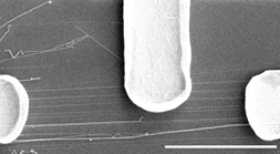 |
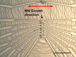
Nanowire electronics: (Top) Optical image shows metal electrodes attached to zinc oxide nanowires using the NIST technique. Dark spots near the center are the gold pads that start nanowire growth; red arrow shows direction of growth. Scale bar is 50 micrometers long. (Bottom) Scanning electron microscope image shows electrodes connected to group of nanowires. Scale bar is five micrometers long.
Credit: NIST
View hi-resolution image (top)
View hi-resolution image (bottom) |
In the growing catalog of nanoscale technologies, nanowires—tiny rows of conductor or semiconductor atoms—have attracted a great deal of interest for their potential to build unique atomic-scale electronics. But before you can buy some at your local Nano Depot, manufacturers will need efficient, reliable methods to build them in quantity. NIST researchers believe they have one solution—a technique that allows them to selectively grow nanowires on sapphire wafers in specific positions and orientations accurately enough to attach contacts and layer other circuit elements, all with
conventional lithography techniques. They detailed their results in a recent paper.*
Despite their name, nanowires are more than just electrical connectors. Researchers have used nanowires to create transistors like those used in memory devices and prototype sensors for gases or biomolecules. However, working with objects only tens of nanometers wide is challenging. A common approach in the lab is to grow nanowires like blades of grass on a suitable substrate, mow them off and mix them in a fluid to transfer them to a test surface, using some method to give them a preferred orientation. When the carrier fluid dries, the nanowires are left behind like tumbled jackstraws. Using scanning probe microscopy or similar tools, researchers hunt around for a convenient, isolated nanowire to work on, or place electrical contacts without knowing the exact positions of the nanowires. It’s not a technique suitable for mass production.
Building on earlier work, NIST researchers used conventional semiconductor manufacturing techniques to deposit small amounts of gold in precise locations on a sapphire wafer. In a high-temperature process, the gold deposits bead up into nanodroplets that act as nucleation points for crystals of zinc oxide, a semiconductor. A slight mismatch in the crystal structures of zinc oxide and sapphire induces the semiconductor to grow as a narrow nanowire in one particular direction across the wafer. Because the starting points and the growth direction are both well known, it is relatively straightforward to add electrical contacts and other features with additional lithography steps.
As proof of concept, the NIST researchers have used this procedure to create more than 600 nanowire-based transistors, a circuit element commonly used in digital memory chips, in a single process. In the prototype process, they report, the nanowires typical grew in small bunches of up to eight wires at a time, but finer control over the size of the initial gold deposits should make it possible to select the number of wires in each position. The technique, they say, should allow industrial-scale production of nanowire-based devices.
*B. Nikoobakht. Toward industrial-scale fabrication of nanowire-based devices. Chem. Mater., ASAP Article 10.1021/cm071798p S0897-4756(07)01798-X. Web release date: October 9, 2007.
Making a Good Impression: Nanoimprint Lithography Tests at NIST
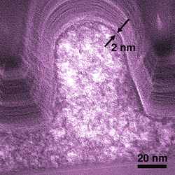 |
Electron micrograph shows a cross section of a typical SOG microcircuit feature. Nanoporous regions in the interior are lighter. The process forms a dense, stronger skin about 2 nanometers thick on the outside. (Color added for clarity.)
Credit: NIST
View hi-resolution image |
In what should be good news for integrated circuit manufacturers, recent NIST studies have helped to resolve two important questions about an emerging microcircuit manufacturing technology called nanoimprint lithography (NIL)—yes, it can accurately stamp delicate insulating structures on advanced microchips, and, no, it doesn’t damage them, in fact it makes them better.
An emerging manufacturing technique, NIL is basically an embossing process. A stamp with a nanoscale pattern in its surface is pressed into a soft film on the surface of a semiconductor wafer. The film is hardened, usually by heating or exposure to ultraviolet light, and the film retains the impressed pattern from the stamp. The process is astonishingly accurate. NIL has been used to create features as small as 10 nanometers across with relatively complex shapes.
NIL is being eyed in particular for building the complexly patterned insulating layers sandwiched between layers of logic devices in future generations of integrated circuits. State-of-the-art semiconductors contain over a billion transistors, packed together into a footprint of silicon that is no bigger than a few square centimeters. Several miles of nanoscale copper wiring are required to connect the devices, and these wires must be separated by a highly efficient insulator. One candidate is a porous glassy material called SOG (for spin-on organosilicate glass) that can be applied as a thin fluid film. When heated, SOG turns into a thin glass film laced with nanometer pores that enhance the electrical insulation. But SOG is relatively delicate, and the conventional photoresist etching process used to cut trenches for the wiring can compromise it. NIL, on the other hand, might be able to pattern SOG layers with wiring trenches and eliminate several time-consuming and expensive photolithography steps if it could pattern the film accurately and do so without destroying the delicate nanopore lacework.
In a paper published in 2007,* NIST materials scientists addressed the first question. Using sensitive X-ray measurements, they demonstrated that NIL could be used on a functional SOG material to transfer patterns with details finer than 100 nanometers with minimal distortion due to the processing. In a new paper,** they extend this work to study the effect of the embossing process on the nanopore structure in the glass. Using a combination of techniques to measure the distribution of nanopores in the insulator material, they found that the NIL embossing process actually has a beneficial effect—it increases the population of small pores, which improve performance, reduces the population of larger pores that can cause problems, and creates a thin, dense protective skin across the surface of the material. All of these effects are highly attractive for minimizing short circuits in semiconductor devices.
Taken together, the two papers suggest that nanoimprint lithography can produce superior nanoporous insulator layers in advanced semiconductor devices with significantly fewer-and easier-processing steps than conventional lithography.
*H.W. Ro, R.L. Jones, H. Peng, D.R. Hines, H-J. Lee, E.K. Lin, A. Karim, D.Y. Yoon, D.W. Gidley and C.L. Soles. The direct patterning of nanoporous interlayer dielectric insulator films by nanoimprint lithography. Advanced Materials. 2007, 19, 2919-2924.
**H.W. Ro, H. Peng, K.-i. Niihara, H.-J. Lee, E.K. Lin, A. Karim, D.W. Gidley, H. Jinnai, D.Y. Yoon and C.L. Soles. Self-sealing of nanoporous low dielectric constant patterns fabricated by nanoimprint lithography. Advanced Materials 2008, Early view: April 15, 2008.
Environment, Health,
and Safety
Study: Cells Selectively
Absorb Short Nanotubes
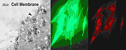 |
Nanotube length threshold: NIST experiments using human lung cells demonstrate that DNA-wrapped single-walled carbon nanotubes longer than about 200 nanometers are excluded from cells while shorter lengths are able to penetrate the cell interior (dark lines in the fluorescence image above).
Credit: NIST
View hi-resolution image |
DNA-wrapped single-walled carbon nanotubes (SWCNTs) shorter than about 200 nanometers readily enter into human lung cells and so may pose an increased risk to health, according to NIST laboratory studies.*
Eyed for uses ranging from electronic displays to fuel cells to water filtration, SWCNTs are tiny cylinders—essentially single-sheet rolls of carbon atoms. They are many times stronger than steel and possess superlative thermal, optical, and electronic properties, but safety and biocompatibility remain an open question.
“Published data citing in vitro (outside the body) toxicity are particularly inconsistent and widely disputed,” writes biomaterials scientist Matthew Becker and his NIST colleagues. Public concerns surrounding the environmental, health, and safety impacts of SWCNTs could derail efforts to fast-track the development of nanotubes for advanced technology applications. A significant hurdle in outlining the parameters contributing to nanotube toxicity is to prepare well-defined and characterized
nanotube samples, as they typically contain a distribution of lengths, diameters, twists, and impurities.
The team chose to isolate the effects of nanotube length. They first adsorbed short DNA molecules onto the nanotubes because this renders them soluble in water and allows them to be sorted and separated by length. The researchers then exposed human lung fibroblasts to solutions containing unsorted nanotubes. Regardless of the concentration levels, the cells did not absorb between about one-fourth and one-third of the SWCNTs in the solutions. Further examination of the results revealed that only short nanotubes made it into the cellular
interior.
In the next phase of the research, the team exposed the cells to sorted nanotubes of controlled length. They found that tubes longer than about 200 nanometers were excluded from the cells and remained in solution. Cells exposed to the longer nanotube solutions did not undergo a decrease in metabolic activity, but cells exposed to nanotubes below that threshold absorbed them and, depending on the concentration level, died or showed other signs of toxicity. “Our results demonstrate that cellular uptake in these lung cells depends significantly on the length of the nanotubes,” Becker explains. “This is the first of many steps in the critical goal of reducing health risk by de novo engineering of the nanotubes themselves.”
*M.L. Becker, J.A. Fagan, N.D. Gallant, B.J. Bauer, V. Bajpai, E.K. Hobbie, S.H. Lacerda, K. B. Migler and J.P. Jakupciak. Length-dependent uptake of DNA-wrapped single-walled carbon nanotubes. Advanced Materials. Published online March 20, 2007.
Carbon Nanotube Measurements: Latest in NIST ‘How-To’ Series
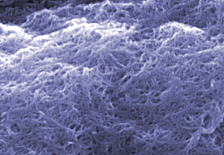 |
Scanning electron microscope image of 'cleaned' carbon nanotubes at NIST (color added for clarity).
Credit: NIST
View hi-resolution image |
NIST, in collaboration with the National Aeronautics and Space Administration (NASA), has published detailed guidelines* for making essential measurements on samples of single-walled carbon nanotubes (SWCNTs). The new guide constitutes the current “best practices” for characterizing one of the most promising and heavily studied of the new generation of nanoscale materials.
Nanotubes are essentially cylinders of carbon atoms with a wall only one atom thick and a diameter of a couple of nanometers—but lengths up to several million times their diameter. (Think of a soup can about 100 kilometers tall.) Because of their unique electronic, thermal, optical, and mechanical properties they are being studied for a wide—and expanding—range of applications, including ultrastrong fibers for nanocomposite materials, circuit elements in molecular electronics, hydrogen storage components for fuel cells, and light sources for compact, efficient flat-panel displays. One basic problem is assuring the quality and purity of SWCNT materials. All known techniques for producing these tiny tubes also produce large quantities of nanojunk: simple graphite and carbon soot often encapsulating small metal particles used to catalyze the nanotube synthesis process.
Accurate, reliable, and preferably rapid measurement techniques are needed to optimize production processes to create more product and fewer impurities. These will help to control cleaning and purifying processes and ultimately to improve the confidence of buyers and sellers of SWCNT materials. The NIST “Recommended Practice Guide” on Measurement Issues in Single Wall Carbon Nanotubes grew out of NIST-NASA workshop held in 2005. It represents what industry, government, and academic researchers regard as the most useful and accurate measurement techniques for characterizing the purity of SWCNT samples. A collaborative effort that includes the United States, China, Japan, and Korea is now under way under the International Organization for Standardization (ISO) to develop these techniques into standards that will help ensure uniform characterization metrics used when buying and selling nanotubes. The editors caution that in the fast-moving field of carbon nanotubes, characterization methods will need to be updated periodically.
The NIST Recommend Practice Guides are a set of publications devoted to specific, challenging measurement issues faced in industry and research. Online copies of Measurement Issues in Single Wall Carbon Nanotubes and other guides in the series are available at the Web site for the “How To Measure” book series: www.nist.gov/public_affairs/practiceguides/practiceguides.htm.
Tools and Methods for Extreme Measurements
NIST Reference Materials Are ‘Gold Standard’ for Bio-Nanotech Research
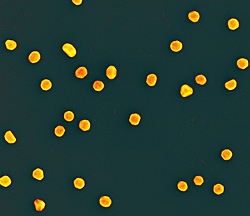 |
Scanning electron micrograph (250,000 times magnification) showing the gold nanoparticles created by NIST and the National Cancer Institute’s Nanotechnology Characterization Laboratory (NCL) for use as reference standards in biomedical research laboratories.
Credit: Andras Vladar, NIST
View hi-resolution image |
NIST has issued its first reference standards for nanoscale particles targeted for the biomedical research community—literally “gold standards” for labs studying the biological effects of nanoparticles. The three new materials, gold spheres nominally 10, 30, and 60 nanometers in diameter, were developed in cooperation with the National Cancer Institute’s Nanotechnology Characterization Laboratory (NCL).
Nanosized particles are the subject of a great deal of biological research. On the positive side, they are being studied as vehicles for targeted drug delivery that have the potential to revolutionize cancer treatments. On the negative side, nanoparticles may pose special toxicity issues. Research in the field has suffered from a lack
of reliable nanoscale measurement standards, both to ensure consistency of data from one lab to the next and to verify the performance of measurement instruments and analytic techniques.
The new NIST reference materials are citrate-stabilized nanosized gold particles in a colloidal suspension in water. They have been extensively analyzed by NIST scientists to assess particle size and size distribution by multiple techniques for dry-deposited, aerosol and liquid-borne forms of the material. Dimensions were measured using six independent methods. At the nanoscale in particular, different measurement techniques can and will produce different types of values for the same particles.
In addition, the new materials have been chemically analyzed for the concentrations of gold, chloride ion, sodium and citrate, as well as pH, electrical conductivity, and zeta potential (a measure of the stability of the colloidal solution).
NCL examines candidate nanotech cancer drugs developed by biotech firms and academic labs. NCL and the NCI’s Alliance for Nanotechnology in Cancer sponsored the NIST work.
Additional technical and ordering information for the new NIST nanoparticle reference materials is available at:
NIST Advancing Nanoscale Research with New Helium Ion Microscope
The first commercially available helium ion microscope—a breakthrough technology that yields once-unattainably high levels of resolution for surface
imaging—has been installed at NIST’s Advanced Measurement Laboratory.
A NIST precision engineering research team is studying the imaging mechanisms and modeling
analytical capabilities and uncertainties regarding dimensional measurements made with the instrument. This work is being done under a cooperative research agreement with Carl Zeiss SMT, manufacturer of the microscope. In addition, International SEMATECH, the consortium of integrated circuit manufacturers, has asked NIST to evaluate HIM for potential measurement and quality control applications in chip manufacturing.
One research project aims to generate highly accurate images of surface topography, surface features, or other nanoscale structures, which, in turn, can be used to calibrate or verify measurements obtained using contact or near-contact scanned probe techniques. Another study will use HIM for imaging and dimensional measurements of nanoparticles in biological systems.
The current suite of detectors on NIST’s HIM can provide information on topographic, material, crystallographic, and electrical properties of the sample.
HIM potentially poses several imaging advantages over traditional scanning electron microscopes (SEMs) currently used in research and manufacturing facilities across the world. Due to the very high source brightness, and the shorter wavelength of the helium ions, it is
theoretically possible to focus the helium ion beam
into smaller probes, enabling dramatic improvement in resolution.
‘Nanodrop’ Test Tubes Created
with a Flip of a Switch
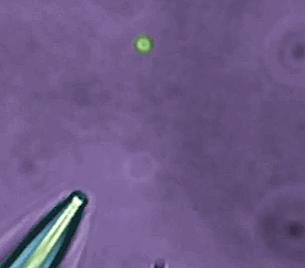 |
With the flip of a switch: Nanodrop ‘test tubes’ are created by an electronic switch that causes a micropipette to jerk back and leave behind a droplet less that 1 micrometer in diameter for study. (WMV video clip requires Windows Media Player (or equivalent), a free download—click here.)
Credit: NIST
View hi-resolution image |
A new device that creates nanodroplet “test tubes” for studying individual proteins under conditions that mimic the crowded confines of a living cell has been demonstrated by NIST researchers. “By confining individual proteins in nanodroplets of water, researchers can directly observe the dynamics and structural changes of these biomolecules,” says NIST physicist Lori Goldner.
Researchers recently have turned their attention to the role that crowding plays in the behavior of proteins and other biomolecules—there is not much extra space in a cell. NIST’s nanodroplets can mimic the crowded environment in cells where the proteins live while providing advantages over other techniques to confine or immobilize proteins for study that may interfere with or damage the protein. This more realistic setting can help researchers study the molecular basis of disease and supply information for developing new pharmaceuticals. For example, misfolded proteins play a role in many illnesses including Type 2 diabetes and Alzheimer’s and Parkinson’s diseases. By seeing how proteins fold in these nanodroplets, researchers may gain new insight into these ailments and may find new therapies.
The NIST nanodroplet delivery system uses tiny glass micropipettes to create tiny water droplets suspended in an oily fluid for study under a microscope. An applied pressure forces the water solution containing protein test subjects to the tip of the micropipette as it sits immersed in a small drop of oil on the microscope stage. Then, like a magician whipping a tablecloth off a table while leaving the dinnerware behind, an electronic switch causes the pipette to jerk back, leaving behind a small droplet typically less than a micrometer in diameter.
The droplet is held in place with a laser “optical tweezer,” and another laser is used to excite fluorescence from the molecule or molecules in the droplet. In one set of fluorescence experiments, explains Goldner, “The molecules seem unperturbed by their confinement.
They do not stick to the walls or leave the container—important facts to know for doing nanochemistry or
single-molecule biophysics.” The team also demonstrated that single fluorescent protein molecules could be detected inside the droplets.
Fluorescence can reveal the number of molecules within the nanodroplet and can show the motion or
structural changes of the confined molecule or molecules, allowing researchers to study how two or more proteins interact. By using only a few molecules and tiny amounts of reagents, the technique also minimizes the need for expensive or toxic chemicals.
*J. Tang, A.M. Jofre, G.M. Lowman, R.B. Kishore, J.E. Reiner, K. Helmerson, L.S. Goldner and M.E. Greene. Green fluorescent protein in inertially injected aqueous nanodroplets. published in Langmuir, ASAP Article, Web release date: March 27, 2008.
Toward Better Materials
NIST Develops Rapid Method for Judging Nanotube Purity
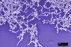 |
A new NIST method for rapidly assessing the quality of carbon nanotubes was evaluated in part by comparing the results to electron micrographs, which revealed uneven composition such as large bundles of nanotubes and impurities such as metallic particles. (Color added.)
Credit: NIST
View hi-resolution image |
Initial tests of a new NIST-developed method for rapidly assessing the quality of carbon nanotubes show that the method not only is faster than the standard analytic technique but also can screen much smaller samples
for purity and consistency and better detect sample
variability.
Carbon nanotubes have unique properties that could be useful in fields such as aerospace, microelectronics, and biotechnology. However, these properties may vary widely depending on nanotube dimensions, uniformity, and chemical purity. Nanotube samples typically contain a significant percentage of more ordinary forms of carbon as well as metal particles left over from catalysts used in manufacturing. The new NIST method* involves spraying nanotube coatings onto a quartz crystal, gradually heating the coated crystal, and measuring the change in its resonant frequency as different forms of carbon vaporize. The frequency changes in proportion to the mass of the coating, and scientists use this as a measure of stability at different temperatures to gauge consistency among samples. The quartz crystal technique, which can reveal mass changes of just a few nanograms, already is used in other contexts to detect toxic gases and measure molecular interactions.
NIST researchers tested dozens of samples from a batch of commercial single-walled carbon nanotubes, comparing results of the new method with those from a standard technique, thermogravimetric analysis, and confirming results with scanning electron microscopy. Both methods revealed that the samples contained large amounts of amorphous carbon as well as residual metal particles. But the quartz crystal method could obtain results from just micrograms of material, compared to milligrams for thermogravimetric analysis, and also revealed several orders of magnitude more variability in the samples tested. The new technique also uses simpler equipment.
Although the differences among nanotube samples may appear subtle, they may still affect product viability, because even small variations in material composition can affect electrical and thermal behavior, and lack of uniformity may demand higher loads of nanotubes, which are expensive. NIST scientists carried out the tests with the help of students from the University of Colorado-Boulder and Rensselaer Polytechnic Institute.
*S.A. Hooker, R. Geiss, R. Schilt, and A. Kar. Rapid inspection of carbon nanotube quality. Paper presented Jan. 25, 2007, at the 31st International Cocoa Beach Conference and Exposition on Advanced Ceramics and Composites, Daytona Beach, Fla.
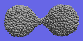
Nanomaterials Show Unexpected Strength Under Stress
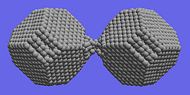 |
NIST researchers have shown that substances such as silica that are brittle in bulk exhibit ductile behavior at the nanoscale. Computer simulations demonstrate the material extension and necking that occurs during the separation of amorphous (top) and crystalline (bottom) silica nanoparticles.
Credit: NIST
View hi-resolution image of top image
View hi-resolution image of bottom image |
In yet another twist on the strangeness of the nanoworld, researchers at NIST and the University of Maryland-College Park have discovered that materials such as silica that are quite brittle in bulk form behave as ductile as gold at the nanoscale. Their results may affect the design of future nanomachines.
NIST scientists Pradeep Namboodiri and Doo-In Kim and colleagues first demonstrated* the latest incongruity between the macro and nano worlds this past fall with direct experimental evidence for nanoscale ductility. In a new paper,** presented at the March 2008 meeting of the American Physical Society, NIST researchers Takumi Hawa and Michael Zachariah and guest researcher Brian Henz shared the insights they gained into the phenomenon through their computer simulations of nanoparticle aggregates.
At the macroscale, the point at which a material will fail or break depends on its ability to maintain its shape when stressed. The atoms of ductile substances are able to shuffle around and remain cohesive for much longer than their brittle cousins, which contain faint structural flaws that act as failure points under stress.
At the nanoscale, these structural flaws do not exist, and hence the materials are nearly “perfect.” In addition, these objects are so small that most of the atoms that comprise them reside on the surface. According to Namboodiri and Kim, the properties of the surface atoms, which are more mobile because they are not bounded on all sides, dominate at the nanoscale. This dominance gives an otherwise brittle material such as silica its counterintuitive fracture characteristics.
“The terms ‘brittle’ and ‘ductile’ are macroscopic terminology,” Kim says. “It seems that these terms don’t apply at the nanoscale.”
Using an atomic force microscope (AFM), Kim and Namboodiri were able to look more closely at interfacial fracture than had been done before at the nanoscale. They found that the silica will stretch as much as gold or silver and will continue to deform beyond the point that would be predicted using its bulk-scale properties.
Hawa, Henz, and Zachariah’s simulations reaffirmed their study and added some additional details. They showed that both nanoparticle size and morphology—whether the material is basically crystalline or amorphous, for example—have an effect on the observed
ductility and tensile strength because those factors influence the mobility of surface atoms. In the simulations, the smaller the particles in the aggregate the more ductile the material behaved. Crystalline structures exhibited greater strength when stressed and deformed long after the critical yield point observed macroscopically.
Namboodiri explained that although the work is very basic, these findings might one day inform the design of microelectronic mechanical devices.
*N. Pradeep, D-I. Kim, J. Grobelny, T. Hawa, B. Henz, and M. R. Zachariah. Ductility at the nanoscale: Deformation and fracture of adhesive contacts using atomic force microscopy. Applied Physics Letters, published online 15 November 2007.
**T. Hawa, B. Henz, and M. Zachariah. Computer simulations of nanoparticle aggregate fracture. Presented Wednesday, March 12, 2008, at the 2008 APS meeting in New Orleans, La.
Shear Ingenuity: Tweaking the Conductivity of Nanotube Composites
 |
Confocal microscope image of a carbon nanotube/polypropylene composite. Small concentrations of carbon nanotubes–here about 1 percent by mass–can change the electrical properties of the polymer dramatically.
Credit: NIST
View hi-resolution image |
One of the immediate applications of carbon nanotubes (CNT) is as an additive to polymers to create
electrically conducting plastics—a relatively low CNT concentration can dramatically change the polymer’s electrical conductivity by orders of magnitude, from an insulator to a conductor. New measurements by NIST scientists have uncovered an intriguing wrinkle. For a given CNT concentration, the electrical properties of the composite can be tuned from being a conductor to a non-conductor simply by changing processing conditions—basically how fast the polymer flows.
Carbon nanotubes—sheets of graphite rolled up into nanoscale hollow cylinders—are under intense scrutiny for a wide range of materials applications. The NIST study* shows how the conductivity and dielectric properties of these mixtures depend on flow and how they change once flow has stopped. These property changes have relevance to the process design of these materials in a long list of potential applications for conducting plastics, including transparent electrodes, antennas, electronic packaging, sensors, automotive paint, anti-static fuel hoses, and aircraft components.
The NIST researchers augmented a standard instrument, a shear rheometer, normally used for viscosity measurements, to simultaneously measure conductivity and dielectric properties. Using this “rheo-dielectric spectrometer,” they discovered that the conductivity of the nanocomposite dramatically decreases with increasing flow rate, effectively changing the material from a conductor to an insulator. This extraordinary sensitivity of the conductivity (and other properties)
to flow is prevalent
near a
characteristic CNT concentration where an interpenetrating CNT network first forms. Surprisingly, once the flow is removed, they found that the nanocomposite reverts back to its original conductivity.
Based on these measurements, the NIST team proposed a theoretical model that successfully accounts for these dramatic effects. This model quantitatively predicts the observed conductor-insulator transition and is useful for optimizing and controlling the properties of these new polymer-nanotube composites.
*J. Obrzut, J.F. Douglas, S.B. Kharchenko and K. B. Migler. Shear-induced conductor-insulator transition in melt-mixed polypropylene-carbon nanotube dispersions. Physical Review B 76, 195420-2007. Nov. 15, 2007.
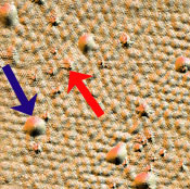
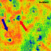
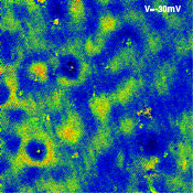
Speed Bumps Less Important
Than Potholes for Graphene
For electrical charges racing through an atom-thick sheet of graphene, occasional hills and valleys are no
big deal, but the potholes—single-atom defects in the crystal—they’re killers. That’s one of the conclusions reached by researchers from NIST and the Georgia Institute of Technology, who created detailed maps of electron interference patterns in graphene to understand how defects in the two-dimensional carbon crystal affect charge flow through the material. The new results*
have implications for the design of graphene-based nanoelectronics.
A single layer of carbon atoms tightly arranged in a honeycomb pattern, graphene was long thought to be an interesting theoretical concept that was impossible in practice because it was thought to be too unstable. The discovery, in 2004, that graphene actually could exist touched off a rush of experimentation to explore its properties. Graphene has been described as a carbon nanotube unrolled, and shares some of the unique properties of nanotubes. In particular, it’s a so-called ballistic conductor, meaning that electrons flow through it at high speed with virtually no collisions with atoms in the crystal. This makes it a potentially outstanding conductor for wires and other elements in nanoscale electronics.
Defects or irregularities in the graphene crystal, however, can cause the electrons to bounce back or scatter, the equivalent of electrical resistance, so one key issue is just what sort of defects cause scattering, and how much? To answer this, the NIST-Georgia Tech team grew layers of graphene on wafers of silicon carbide crystals and mapped the sheets with a custom-built scanning tunneling microscope (STM) in the NIST Center for Nanoscale Science and Technology. The instrument can measure both physical surface features and the interference patterns caused by electrons scattering in the crystal. (Graphene on silicon carbide is a leading candidate for graphene-based nanoelectronics.)
The results are counterintuitive. Irregularities in the underlying silicon carbide cause bumps and dips in the graphene sheet that lies over it rather like a blanket on a lumpy bed, but these relatively large bumps have only a minor effect on the electron’s passage. In contrast, missing carbon atoms in the crystal lattice cause strong scattering, the interference patterns rippling around them like waves hitting the piles of a pier. From a detailed analysis of these interference patterns, the team verified that electrons in the graphene sheet behave like photons, even at the nanometer scale.
This work is supported in part by the Office of Naval Research, National Science Foundation and Intel Research.
*G.M. Rutter, J.N. Crain, N.P. Guisinger, T. Li, P.N. First and J.A. Stroscio. Scattering and interference in epitaxial graphene. Science. July 13, 2007.
Paving the Way for
Next-Generation Devices
Copolymers Block Out New Approaches to Microelectronics
In response to the electronics industry’s rallying cry of “smaller and faster,” the next breakthroughs in the electronics size barrier are likely to come from microchips and data storage devices created out of novel materials such as organic molecules and polymers. Recent accomplishments at NIST are helping to move these new materials closer to practical applications.
In March 2008, NIST researchers reported how
they have improved manipulation of so-called block copolymers—polymers made of a mixture of two or more different molecule building blocks that are tethered at a junction point—which can form arrays of tiny dots that could be used as the basis for electronic components that pack terabytes (1,000 gigabytes) of memory in something as small as a pack of gum.
One of the challenges in polymer nanotechnology is how to control their self-assembly—a hard-to-control process for materials that require precision. An important recent NIST accomplishment has been in developing accurate measurements of thin film polymeric nanostructure in 3-D. Ron Jones, together with colleagues from NIST, the University of Maryland, and IBM, has used NIST’s neutron scattering and reflectivity facility to deflect neutrons off block copolymer films from many different angles. By combining the many 2-D neutron scattering pictures into a single composite scattering pattern, this technique provides the first quantitative method for imaging the 3-D internal structure of thin film polymeric nanostructures using neutron scattering—a crucial tool to see if the nanoscale polymer structures are in their required positions.1
NIST researchers also have developed new insights on how best to nudge these self-assembling materials into those positions. Their computer simulations show how the polymers assemble when they are placed on templates lined with troughs separated by crests.2 When a heated zone is swept across the template, the polymer molecules assemble into almost defect-free, well-aligned lines faster over the entire template, an important feature for nanotech manufacturing applications.3 Meanwhile, collaborators from NIST, IBM, and the University of Maryland have found that changing the surface chemistry of the template by making some parts hydrophillic and some parts hydrophobic also can elegantly control the dimension of the block-copolymer pattern relative to the chemical template.4
Sometimes, however, the emphasis on precise placement may be overstated. NIST researcher Kevin Yager has learned that sloppiness has its merits. By purposely roughening up his templates with a sprinkling of chemically modified nanoparticle silica, he has forced block copolymers into standing perpendicular to the template—a feat that is generally considered tough to manage but important for nanotech applications.5 Of course, the inner structure of the polymers are not orderly with this technique, but for those applications where only the surface needs to be smooth, this is an ideal, inexpensive way to achieve vertical structures.
1 R. Jones, X. Zhang, S. Kim, A. Karim, R. Briber and H. Kim. Orientation distribution for thin film block copolymers. Presented at the March Meeting of the American Physical Society, March 12, 2008, New Orleans, La.
2 A. Bosse, R. Jones and A. Karim. Fluctuation-induced line-edge roughness in nano-confined block copolymer thin films. Presented at the March Meeting of the American Physical Society, March 11, 2008, New Orleans, La.
3 A. Karim. INVITED TALK. Templated Self-Assembly of Block Copolymer Thin Films. Presented at the March Meeting of the American Physical Society, March 10, 2008, New Orleans, La.
4 S. Kim, H-J. Lee, R.L. Jones, A. Karim, R.M. Briber and
H-C. Kim. Precise control of 3-dimensional block copolymer assembly using 2-dimensional chemical templates. Presented at the March Meeting of the American Physical Society, March 10, 2008, New Orleans, La.
5 K. Yager, A. Karim and E. Amis. Disordered nanoparticle interfaces for defect-tolerance in the self-assembly of block-copolymers. Presented at the March Meeting of the American Physical Society, March 12, 2008, New Orleans, La.
‘High Q’ NIST Nanowires
May be Practical Oscillators
 |
Electron micrograph of a NIST-grown nanowire with a high “quality factor” vibrating more than 1 million times per second. At lower right, a stationary nanowire shows the typical hexagonal shape of the gallium nitride structures.
Credit: S. Tanner, CU/JILA
View higher resolution image |
Nanowires grown at NIST have a mechanical “quality factor” at least 10 times higher than reported values for other nanoscale devices, such as carbon nanotubes, and comparable to that of commercial quartz crystals. Because a high Q factor indicates a capacity for stable vibrations, the nanowires might be used as oscillators in nanoelectromechanical systems for future nanosensors and communications devices.
“We think the most interesting thing about these wires is the very high quality factor observed for such a small object,” says Kris Bertness, the NIST researcher who grew the nanowires.
NIST has developed a unique way of growing hexagonal gallium nitride (GaN) nanowires featuring low defect density and high luminescence intensity. In a new paper,* researchers at NIST and the University of Colorado at Boulder report high Q factors in wires that are 30 to 500 nanometers in diameter and 5 to 20 micrometers long, vibrating between 400,000 and 2.8 million times per second. (For comparison, the quartz crystals used in watches usually vibrate about 32,000 times a second.) The nanowires vibrated when placed on a piezoelectric device stimulated by an electrical signal. The nanowires also oscillated when excited directly by an electron beam, apparently due to the GaN material’s intrinsic piezoelectric ability to covert voltage to mechanical force.
Q measures the damping of oscillations in a mechanical system as a function of frequency—the higher its Q, the longer a bell rings after being struck. Ordinarily, Q factors of mechanical resonators tend to drop as their diameters shrink. But GaN nanowires have a number of properties that may boost their Q and make them suitable as practical oscillators. GaN also has a resonant frequency similar to silicon (commonly used in microelectronics) but is less susceptible to some sources of “noise.” Finally, GaN has high heat capacity and thermal conductivity, reducing sensitivity to temperature fluctuations. Another practical advantage is that NIST’s GaN nanowires are grown on silicon, making them compatible with existing microelectronics processing methods.
To measure the resonance properties of the nanowires, researchers observed clumps of nanowires using a scanning electron microscope. As the
frequency of the applied signal was varied across a range, the nanowires seen in micrographs appear to blur or fan out at or near the resonance frequency. For the nanowire shown in the image, the Q value (about 38,000) is at least 10 times higher than previously reported values for other GaN nanowires,
carbon nanotubes, and single-crystal silicon microstructures of similar surface-to-volume ratio. The researchers have measured Q values of more than 1 million in resonating GaN nanowires using feedback (like continuous striking of a bell to keep it ringing), as would occur in a real device.
*S.M. Tanner, J.M. Gray, C.T. Rogers, K.A. Bertness, and N.A. Sanford. High-Q GaN Nanowire Resonators and Oscillators. Applied Physics Letters. 91, 203117 (2007).
New Fabrication Technique
Yields Nanoscale UV LEDs
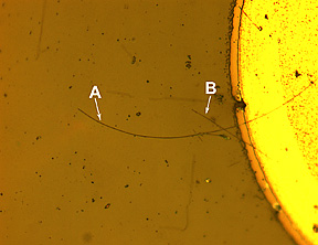 |
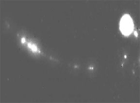 |
[Top] Micrograph of a complete nanowire LED with the end contact. The long nanowire (A) is about 110 micrometers long, a shorter nanowire (B) crosses it. The bright circular section is the metal post from which the nanowires are aligned.
View hi-resolution image
[Bottom] Optical image of the same nanowire in action. Most of the light emitted from the device is in the ultraviolet portion of the spectrum, but enough visible light is generated to see it glowing.
View hi-resolution image
Credit: NIST
|
A team of researchers from NIST, the University of Maryland, and Howard University have developed a technique to create tiny, highly efficient light-emitting diodes (LEDs) from nanowires. As described in a recent paper,* the fabricated LEDs emit ultraviolet light—a key wavelength range required for many light-based nanotechnologies, including data storage—and the assembly technique is well-suited for scaling to commercial
production.
Light-based nanoscale devices, such as LEDs, could be important building blocks for a new generation of ultracompact, inexpensive technologies, including sensors and optical communications devices. Ultraviolet LEDs are particularly important for data-storage and biological sensing devices, such as detectors for airborne pathogens. Nanowires made of a particular class of semiconductors that includes aluminum nitride, gallium nitride, and indium nitride are the most promising
candidates for nanoscale LEDs. But, says NIST researcher Abhishek Motayed, “The current nanowire LEDs are created using tedious nanowire manipulation methods and one-by-one fabrication techniques, which makes them unsuitable for commercial realization.”
The NIST team used batch fabrication techniques, such as photolithography (printing a pattern into a material using light, similar to photography), wet etching, and metal deposition. They aligned the nanowires using an electric field, eliminating the delicate and time-consuming task of placing each nanowire separately.
A key feature of the new nanowire LEDs is that they are made from a single compound, gallium nitride (GaN). Each LED consists of an “n-type” GaN nanowire placed on the surface of a “p-type” GaN thin film. “N-type” and “p-type” refer to semiconductors with, respectively, an abundance of electrons and an abundance of positively charged electron vacancies called holes. P-n junctions made from the same basic compound yield more efficient LEDs than those made with different compounds, and so can operate at lower power.
When the proper voltage is applied to the junction, it emits light with a peak wavelength of 365 nanometers, which falls squarely in the ultraviolet range. The group produced and tested more than 40 of these LEDs; all showed very similar emission properties. They also
displayed excellent thermal stability—withstanding
temperatures up to 750 degrees Celsius—and operational stability, showing no signs of deterioration even after two continuous hours of operation at room temperature. These properties indicate that this LED production method yields reliable, stable devices. The researchers say their method could be used to fabricate other nanowire structures as well as applications requiring a large area of nanoscale light sources.
*A. Motayed, A. Davydov, M. He, S. N. Mohammed, and
J. Melngailis. 365 nm operation of n-nanowire/p-gallium nitride homojunction light emitting diodes. Applied Physics Letters 90, 183120 (2007).
Changing the Rings: A Key Finding for Magnetics Design
Researchers at NIST’s Center for Nanoscale Science and Technology (CNST) have done the first theoretical determination of the dominant damping mechanism that settles down excited magnetic states—“ringing” in physics parlance—in some key metals. Their results, published in the Physical Review Letters,* point to more efficient methods to predict the dynamics of magnetic materials and to improve the design of key materials for magnetic devices.
The ability to control the dynamics of magnetic materials is critical to high-performance electronic devices such as magnetic field sensors and magnetic recording media. In a computer’s magnetic storage—like a hard disk—a logical bit is represented by a group of atoms whose electron “spins” all are oriented in a particular direction, creating a minute magnetic field. To change the bit from, say, a one to a zero, the drive’s write head imposes a field in a different direction at that point, causing the electrons to become magnetically excited. Their magnetic poles begin precessing—the same motion seen in a child’s spinning top when it’s
tilted to one side and begins rotating around a vertical axis. Damping is what siphons off this energy, allowing the electron spins to settle into a new orientation. For fast write speeds—magnetization reversals in a nanosecond or faster—a hard disk wants strong damping.
On the other hand, damping is associated with noise and loss of signal in the same drive’s read heads—and other magnetic field sensors—so they need materials with very weak damping.
The design of improved magnetic devices, particularly at the nanoscale, requires a palette of materials with tailored damping rates, but unfortunately the damping mechanism is not well understood. Important damping mechanisms have not been identified, particularly for the so-called intrinsic damping seen in pure ferromagnetic materials, and no quantitative calculations of the
damping rate have been done, so the search for improved materials must be largely by trial and error.
To address this, CNST researchers calculated the expected damping parameters for three commonly used ferromagnetic elements, iron, cobalt, and nickel, based on proposed models that link precession damping in a complex fashion with the creation of electron-hole pairs in the metal that ultimately dissipate the magnetic excitation energy as vibration energy in the crystal structure. The calculation is extremely complex, both because of the intrinsic difficulty of accounting for the mutual interactions of large numbers of electrons in a solid and because the phenomenon is inherently complex, with at least two different and competing mechanisms. Damping rises with temperature in all three metals, for example, but in cobalt and nickel it also rises with decreasing temperature at low temperatures.
By comparing the calculated damping effects with experimental measurements, the team was able to identify the dominant mechanisms behind intrinsic damping in the three metals, which at room temperature and above is tied to electron energy transitions. The results, they say, point to materials design techniques that could be used to optimize damping in new magnetic alloys.
*K. Gilmore, Y.U. Idzerda, and M.D. Stiles. Identification of the dominant precession-damping mechanism in Fe, Co, and Ni by first-principles calculations. Physical Review Letters 99, 027204. July 13, 2007.
For further information
For more information on NIST’s nanotechnology research, facilities, and services, visit www.nist.gov/public_affairs/nanotech.htm or contact inquiries@nist.gov, (301) 975-NIST (6478)
|