|
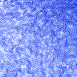 |
Colorized
micrograph of a nanoporous insulation film after “wrinkling”
with a new NIST measurement method.
|
The challenge
of determining whether thin films—some no thicker than
a single molecule—are strong enough for a growing number
of important technology jobs just got easier and quicker thanks
to an inexpensive testing method reported in the upcoming
issue of Nature Materials by a team led
by researchers at the Commerce
Department’s National
Institute of Standards and Technology (NIST).
Useful
for evaluating all types and combinations of materials, the
new method measures and analyzes the strength and stiffness
of a thin-film sample in about 2 seconds, as compared with
several minutes for indentation and other conventional approaches.
In addition, the NIST-developed technique accommodates high-throughput
testing, so that hundreds or even a few thousand systematically
varying samples can be tested in rapid succession.
Accelerated
testing could spur progress in a large variety of existing
and emerging technology areas that rely on thin-film advances
for improved performance or enhanced protection. Examples
include semiconductors, solar cells, fuel cells, coatings,
magnetic storage devices and prospective nanotechnology devices.
For films
less than 1 micrometer thick, mechanical-property measurements
made with existing tools often yield relative values, which
can blur predictions of how different films will perform.
In contrast, the new method yields quantitative measurement
results that permit definitive comparisons between samples.
In the
article,* NIST and IBM collaborators report on how they used
the innovative “measurement platform” to assess
the strength of polymer and ceramic films ranging from a few
nanometers to a micrometer in thickness. One pilot-tested
film was a ceramic material dotted with nanometer-scale pores.
Such nanoporous films are being developed to insulate devices
and layers on future-generation integrated circuits.
While
the nanopores in the so-called low-dielectric-constant (low-k)
films improve their effectiveness as electrical insulators,
the tiny holes also can compromise the films’ strength.
A major concern is whether the nanoporous films can withstand
the rigors of the chemical mechanical polishing process used
to smooth each layer in a chip.
Using
the desk-top testing platform, smaller than a box of tissues,
the team evaluated a battery of low-k films that
varied in porosity, from samples with no pores to samples
in which pores made up half the volume. After comparing the
results with those obtained with the widely used nanoindentation
method, the team concluded that the NIST-developed approach
“provides an inexpensive, fast, and highly effective
technique” for evaluating new varieties of low-k
materials.
“We
expect that this technique will find application in addressing
a variety of questions ranging from fundamental materials
science to applied discovery in the field of films and coatings,”
they write.
Christopher
Stafford, a NIST polymer scientist, suggests other applications
include evaluations of new photoresist masks that will be
used to print chips with the smaller-wavelength ultraviolet
light sources that the semiconductor industry is now implementing.
It also should be useful for assessing the mechanical properties
of nanotechnology devices made with still-experimental methods,
such as nanoimprint lithography in which nanometer-scale features
are stamped into a substrate.
“This
simple technique can provide invaluable information concerning
the mechanics of nanostructured materials and ultrathin polymer
films,” said Stafford.
Called
SIEBIMM (for strain-induced elastic buckling instability for
mechanical measurements), the new method builds on the science
of buckling, which for most of its 400 years has been concerned
with crumbling buildings or crumpling of the Earth’s
crust.
The method
entails mounting a postage-stamp-sized assortment of incrementally
varying thin films on a strip of silicone rubber about the
size of a Band-Aid. The combination of sample array and soft
substrate are placed on a custom-built stage that can be stretched
or compressed.
Subjected
to a gradually increasing force that stretches or squeezes,
a sample becomes unstable and buckles, wrinkling like a piece
of corrugated cardboard. Situated beneath the stage, a laser
beams through the sample and a camera captures the light scattered
at this critical point of instability.
From
the resulting diffraction pattern, the buckling wavelength,
or distance between the peaks of adjacent wrinkles, is determined.
Through a series of mathematical calculations, the buckling
wavelength can be related directly to the elastic modulus
of the sample, which corresponds to the strength of the material.
The SIEBIMM
method was developed at the NIST Combinatorial Methods Center
(www.nist.gov/combi),
which develops rapid, high-throughput technologies to accelerate
the discovery and application of new materials.
As a
non-regulatory agency of the U.S. Department of Commerce’s
Technology Administration, NIST develops and promotes measurement,
standards and technology to enhance productivity, facilitate
trade and improve the quality of life.
-30-
* “A
buckling-based metrology for measuring the elastic moduli of
polymeric thin films,” available at Nature Materials,
Advance Online Publication (AOP): http://www.nature.com/naturematerials.
 Go
back to NIST News Page Go
back to NIST News Page
|