


Electronic Materials and Devices
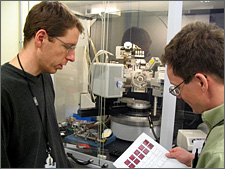
NREL's scientists, Maikel van Hest and John Perkins, discuss x-ray diffraction data from the Bruker D8 Discovery
The Electronic Materials and Devices Project conducts research in semiconductor materials, device properties, and fabrication processes to improve the efficiency, stability, and cost of photovoltaic solar energy conversion. Our research can be characterized three ways: 1) we assist industry in addressing current problems; 2) we explore specific techniques and processes to develop and transfer technology improvements that industry will soon need; and 3) we create new technologies and lead the development of the knowledge base and tools for the future of PV.
Our project is composed of four primary tasks to exploit the numerous opportunities in this fast growing area of photovoltaic research: Silicon Materials, Process and Advanced Concepts, Thin-Film Polycrystalline Compounds, and Concentrator Crystalline Cells. Our management task coordinates project planning and operations within the PV Subprogram and interactions with projects of related interests from other agencies and private sources.
Project Objectives
- Further the fundamental understanding and implementation of performance-enhancing features of low-cost, high-efficiency crystalline silicon (c-Si) and thin-film silicon solar cells.
- Explore new process approaches such as combinatorial science, ink-based electronic materials deposition and hybrid nanostructures for solar energy conversion.
- Adapt NREL's high-efficiency copper indium gallium diselenide (CIGS) and cadmium telluride (CdTe) solar cell materials and systems to allow implementation in low-cost manufacturing, leading to durable performance.
- Develop ultra-high-efficiency solar cells that form the heart of solar concentrator systems to increase performance and reduce system costs.
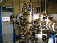
The Riber molecular beam epitaxy provides a key capability for growth of high quality electronic materials.
Project Accomplishments
- Achieved a record efficiency for p-wafer silicon heterojunction solar cells with a confirmed efficiency of 18.2%. This 1 cm2 cell has a-Si contacts on both sides and an open-circuit voltage of 0.667 V.
- Developed a new method for producing thin crystal Si layers by using a scalable hot-wire chemical vapor deposition (CVD) technique to deposit 11 microns of epitaxial Si at 110 nm/min on a Si wafer at the glass-compatible temperature of 615°C. With quality improvements and a suitable seed layer on glass, this technique could be used to develop thin crystal Si layers on inexpensive substrates.
- Developed new combinatorial capabilities for Raman, work function, deposition, and elemental analysis.
- Applied for six patents on the direct printing of precursors for copper indium diselenide (CIS) solar cell absorbers and metallization for Si solar cell contacts.
- Developed state-of-the-art infrastructure for organic photovoltaics (OPV). Obtained a 4.2%-efficient bulk heterojunction cell and >3% inverted OPV solar cells using ZnO anodes.
- Achieved 19.52%-efficient CIGS/CdZnS solar cells.
- Achieved 17.1%-efficient, 1-µm, thin CIGS solar cell and 15.02%-efficient thin CdTe cells.
- Created Cd1-xMgxTe/CdS solar cells for tandem cell applications.
- Lowered series resistance of inverted three-junction cells for 40% performance under concentration.
- Demonstrated GaInNAs 1-eV cells with good depletion widths for use in four-junction cells.
- Achieved record efficiency in lattice-mismatched GaAsP on silicon for low-cost multijunction cells.
Future Project Plans
- Use our improving heterojunction passivation and contacting technologies in a variety of device configurations once single-crystal efficiencies on both n-a and p-type wafers are brought near 20%. This technology can be particularly valuable on multicrystalline and thin crystal silicon materials and in interdigitated cell configurations.
- Grow epitaxial Si layers and solar cells on a variety of Si seed layers on glass to test the viability of our epitaxy at glass-compatible temperatures.
- Transfer Si ink technology and develop 10% CIS solar cell from solution precursors.
- Develop improved polymers for OPV and address interface issues to achieve a 6% solar cell.
- Install and operate polycrystalline thin-film cluster tool in the S&TF.
- Achieve >40% efficiency concentrator solar cell.
- Initiate partnerships with awardees in the Solar America Initiative.
Contact Us
For research and development questions, contact:
John Benner
Email: John_Benner@nrel.gov