| April 29, 2008

[NIST Tech Beat Search] [Credits] [NIST Tech Beat Archives] [Media Contacts] [Subscription Information]

New 3-D Test Method for Biomaterials ‘Flat Out’ Faster
 |  |
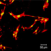 |
Confocal microscope images show how growth and adhesion of bone cells differ across a subset of 3-D scaffolds made with systematically varying blends of ingredients. Red indicates actin filaments, a cytoskeletal protein, and yellow indicates a cell nucleus.
Credit: NIST
View hi-resolution image |
A novel, three-dimensional (3-D) screening method for analyzing interactions between cells and new biomaterials could cut initial search times by more than half, researchers from the National Institute of Standards and Technology (NIST) and Rutgers University report in the new issue of Advanced Materials.* The technique, an advance over flat, two-dimensional screening methods, enables rapid assessment of the biocompatibility and other properties of materials designed for repairing—or even rebuilding—damaged tissues and organs.
In what may be a first, the team demonstrated how to screen cell–material interactions in a biologically representative, but systematically altered, 3-D environment. The pivotal step in the experiment was the collaborators’ success in making so-called libraries of miniature porous scaffolds that are bone-like in structure but vary incrementally in chemical composition. Knowing how changes in scaffold ingredients influence cell responses, researchers can devise strategies for developing biomaterials optimized for particular therapies and treatments.
Until now, attempts to accelerate screening of candidate biomaterials have used flat films and surfaces. (See, for example, “Designer Gradients Speed Surface Science Experiments,” Tech Beat June 8, 2006.) Along with other shortcomings, these two-dimensional substrates are neither consistent with cells’ normal 3-D environment inside the body nor with the most common intended use of biomaterials: creating scaffolds to encourage the growth of cells into functional 3-D tissues and organs.
“Cells are very sensitive to the texture, shapes, and other three-dimensional features of their local environment inside the body,” explains NIST biomaterial scientist Carl Simon. “The large difference in structure between 2-D films and 3-D scaffolds should be considered when screening new materials.”
On a series of plates, each about the size of a dollar bill and arrayed with 96 scaffolds the size of pencil erasers, the researchers conducted the equivalent of 672 individual tests. In all, the tests yielded data for eight separate but related investigations, each one using libraries of 36 incrementally varying scaffolds and 12 controls. On each plate, tests were performed concurrently.
The six cell-culture investigations and two studies of scaffold structure were completed in six days, as compared with 24 days for the traditional method of preparing and testing each sample individually.
In the cell culture experiments, the team analyzed how variations in the chemical makeup of the tiny scaffolds affected the ability of bone-building cells called osteoblasts to multiply and to adhere to scaffolds. The scaffold libraries were made by blending varying proportions of two different compounds prepared at Rutgers based on the amino acid tyrosine, which is a component of proteins found in hair, skin, and other parts of the body.
The project yielded a unique data set, where two materials have been tested side by side in both 2-D and 3-D. In this case, results with 2-D films were predictive of the trends observed with 3-D scaffolds. Further work is required to determine if this will hold true for other cell-material systems.
This research was supported by NIST and the National Institutes of Health.
* Y. Yang, M. L. Becker, D. Bolikal, J. Kohn, D. N. Zeiger and C. G. Simon, Jr. Combinatorial polymer scaffold libraries for screening cell-biomaterial interactions in 3-D. Advanced Materials, 2008, 20, 1–7. (Published on line here.)
Media Contact: Mark Bello, mark.bello@nist.gov, (301) 975-3776 
Making a Good Impression: Nanoimprint Lithography Tests at NIST
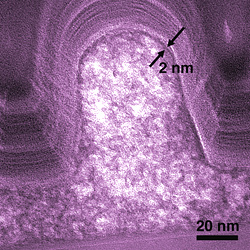 |
Electron micrograph shows a cross-section of a typical SOG microcircuit feature. Nanoporous regions in the interior are lighter. The process forms a dense, stronger skin about 2 nanometers thick on the outside. (Color added for clarity.)
Credit: NIST
View hi-resolution image |
In what should be good news for integrated circuit manufacturers, recent studies by the National Institute of Standards and Technology (NIST) have helped resolve two important questions about an emerging microcircuit manufacturing technology called nanoimprint lithography—yes, it can accurately stamp delicate insulating structures on advanced microchips, and, no, it doesn’t damage them, in fact it makes them better.
An emerging manufacturing technique, nanoimprint lithography (NIL) is basically an embossing process. A stamp with a nanoscale pattern in its surface is pressed into a soft film on the surface of a semiconductor wafer. The film is hardened, usually by heating or exposure to ultraviolet light, and the film retains the impressed pattern from the stamp. The process is astonishingly accurate. NIL has been used to create features as small as ten nanometers across with relatively complex shapes.
NIL is being eyed in particular for building the complexly patterned insulating layers sandwiched between layers of logic devices in future generations of integrated circuits. State-of-the-art semiconductors contain over a billion transistors, packed together into a footprint of silicon that is no bigger than a few square centimeters. Several miles of nanoscale copper wiring are required to connect the devices, and these wires must be separated by a highly efficient insulator. One candidate is a porous glassy material called SOG* that can be applied as a thin fluid film. When heated, SOG turns into a thin glass film laced with nanometer pores that enhance the electrical insulation. But SOG is relatively delicate, and the conventional photoresist etching process used to cut trenches for the wiring can compromise it. NIL, on the other hand, might be able to pattern SOG layers with wiring trenches and eliminate several time-consuming and expensive photolithography steps if it could pattern the film accurately and do so without destroying the delicate nanopore lacework.
In a paper published last fall,** NIST materials scientists addressed the first question. Using sensitive X-ray measurements they demonstrated that NIL could be used on a functional SOG material to transfer patterns with details finer than 100 nanometers with minimal distortion due to the processing. In a new paper this month,*** they extend this work to study the effect of the embossing process on the nanopore structure in the glass. Using a combination of techniques to measure the distribution of nanopores in the insulator material, they found that the NIL embossing process actually has a beneficial effect—it increases the population of small pores, which improve performance, reduces the population of larger pores that can cause problems and creates a thin, dense protective skin across the surface of the material. All of these effects are highly attractive for minimizing short circuits in semiconductor devices.
Taken together, the two papers suggest that nanoimprint lithography can produce superior nanoporous insulator layers in advanced semiconductor devices with significantly fewer—and easier—processing steps than conventional lithography.
* “Spin-on organosilicate glass”
** H.W. Ro, R.L. Jones, H. Peng, D.R. Hines, H-J. Lee, E.K. Lin, A. Karim, D.Y. Yoon, D.W. Gidley and C.L. Soles. The direct patterning of nanoporous interlayer dielectric insulator films by nanoimprint lithography. Advanced Materials. 2007, 19, 2919–2924.
*** H.W. Ro, H. Peng, K.-i. Niihara, H.-J. Lee, E.K. Lin, A. Karim, D.W. Gidley, H. Jinnai, D.Y. Yoon and C.L. Soles. Self-sealing of nanoporous low dielectric constant patterns fabricated by nanoimprint lithography. Advanced Materials 2008, Early View: April 15, 2008.
Media Contact: Michael Baum, michael.baum@nist.gov, (301) 975-2763
High-Flying Electrons May Provide New Test of Quantum Theory
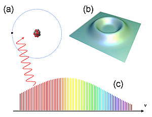 |
(a) In a Rydberg atom, an electron (black dot) is far away from the atomic nucleus (red and grey core). (b) Probability map for an electron in a Rydberg atom shows that it has virtually no probability of being near the nucleus in the center. (c) An optical frequency comb for producing ultraprecise colors of light can trigger quantum energy jumps useful for accurately measuring the Rydberg constant.
Credit: NIST
View hi-resolution image |
Researchers at the National Institute of Standards and Technology (NIST) and Max Planck Institute for Physics in Germany believe they can achieve a significant increase in the accuracy of one of the fundamental constants of nature by boosting an electron to an orbit as far as possible from the atomic nucleus that binds it. The experiment, outlined in a new paper,* would not only mean more accurate identifications of elements in everything from stars to environmental pollutants but also could put the modern theory of the atom to the most stringent tests yet.
The physicists’ quarry is the Rydberg constant, the quantity that specifies the precise color of light that is emitted when an electron jumps from one energy level to another in an atom. The current value of the Rydberg constant comes from comparing theory and experiment for 23 different kinds of energy jumps in hydrogen and deuterium atoms. Researchers have experimentally measured the frequencies of light emitted by these atomic transitions (energy jumps) to an accuracy of as high as 14 parts per quadrillion (one followed by 15 zeros), but the value of the Rydberg constant is known only to about 6.6 parts in a trillion—500 times less accurate. The main hurdle to a more accurate value comes from uncertainties in the size of the atom’s nucleus, which can alter the electron’s energy levels and therefore modify the frequency of light it emits. Another source of uncertainty comes from the fact that electrons sometimes emit and reabsorb short-lived “virtual photons,” a process that also can slightly change the electron’s energy level.
To beat these problems, NIST physicist Peter Mohr and his colleagues propose engineering so-called hydrogen-like Rydberg atoms—atomic nuclei stripped of all but a single electron in a high-lying energy level far away from the nucleus. In such atoms, the electron is so far away from the nucleus that the latter’s size is negligible, and the electron would accelerate less in its high-flung orbit, reducing the effects of “virtual photons” it emits. These simplifications allow theoretical uncertainties to be as small as tens of parts in a quintillion (one followed by 18 zeros).
NIST researchers Joseph Tan and colleagues hope to implement this approach experimentally in their Electron Beam Ion Trap Facility. The idea would be to strip an atom of all its electrons, cool it and inject a single electron in a high-flying orbit. Then the researchers would use a sensitive measurement device known as a frequency comb to measure the light absorbed by this Rydberg atom. The result could be an ultraprecise frequency measurement that would yield an improved value for the Rydberg constant. Such a measurement would be so sensitive that it could reveal anomalies in quantum electrodynamics, the modern theory of the atom.
* U.D. Jentschura, P.J. Mohr, J.N. Tan and B.J. Wundt, Fundamental constants and tests of theory in Rydberg states of hydrogen-like ions, Physical Review Letters, 100, 160404 (2008), posted online April 22, 2008.
Media Contact: Ben Stein, bstein@nist.gov, (301) 975-3097
NIST World Metrology Day Forum Focuses on Anti-Doping Advances
Thomas Hicks won the 1904 Olympic Games marathon in St. Louis, Mo., with a little help from his friends—two doses of strychnine, raw eggs and a brandy chaser, administered during the race! Times have changed. The National Institute of Standards and Technology (NIST) will celebrate World Metrology Day on May 20 with a look at how the science of measurement plays a critical role in enforcing today’s stringent anti-doping rules. A NIST symposium “Metrology for the Olympic Games” in Gaithersburg, Md., will emphasize the measurement research and standards that underpin testing for performance enhancing drugs.
Speakers will include Victoria Ivanova, scientific project manager at the World Anti-Doping Agency (WADA) in Montreal, Canada and Lindsey Mackay, chemical reference methods team leader in the chemical and biological branch of the Innovation, Industry Science and Research of National Measurement Institute of Australia (NIMA).
Ivanova’s overview of WADA testing and research program will review recent drug detection advances including detection methods for various types of blood doping that can increase stamina and performance at the risk of health complications ranging from heart disease, stroke and cerebral or pulmonary embolisms to autoimmune diseases. WADA also is searching for a way to detect emerging threats such as gene doping in which genes could be introduced into an athlete’s body to alter their genetic makeup and improve their physical performance.
Mackay will review NIMA’s work with WADA to provide quality assurance and measurement reference tools for sports testing. NMIA’s anti-doping efforts include work to detect erythropoietin (a natural occurring hormone that increases endurance by increasing the supply of red blood cells), human growth hormone, and artificial or natural steroids.
The International Bureau of Weights and Measures (BIPM) established May 20 as World Metrology Day three years ago and encouraged national measurement institutes such as NIST to celebrate metrology and its importance to society. World Metrology Day commemorates the signing of the Metre (Meter) Convention in 1875. This year’s worldwide theme is “Metrology Measurement in Sports.” Belinda Collins, director of the NIST Technology Services Organization, will give an overview of World Metrology Day. The symposium also will feature poster exhibits on NIST research in sports-related metrology.
Additional detail and registration information is available at www.nist.gov/public_affairs/confpage/080520.htm.
Media Contact: John Blair, john.blair@nist.gov, (301) 975-4261
NIST Signs Cooperative Agreement with U-Albany Nano College
On April 21, the National Institute of Standards and Technology (NIST) signed a Memorandum of Understanding (MOU) with the College of Nanoscale Science and Engineering (CNSE) of the University at Albany-State University of New York, laying the groundwork for future cooperative efforts to develop science and technology for measuring materials at the nanometer scale as well as creating new standards for nanomanufacturing.
NIST Deputy Director James M. Turner, CNSE Vice President and Chief Administrative Officer Alain E. Kaloyeros and Senator Charles E. Schumer (D-N.Y.) participated in the signing ceremony hosted by Senator Schumer at CNSE’s Albany NanoTech Complex, a $4.2 billion, 42,000 square-meter facility that houses more than 2,000 employees including many from the semiconductor industry.
As a result of the MOU, NIST and CNSE will establish policies and general procedures for cooperating and coordinating efforts in areas of common interest. Developing state-of-the-art nanoscale measurement tools and standards is necessary for creating ever-smaller computer chips that perform tasks more quickly and reduce power consumption for a wide range of electronic devices from cell phones to desktop computers.
“Our shared aim is to develop the measurement science infrastructure that is absolutely essential to U.S. innovation and economic competitiveness in nanotechnology,” said NIST Deputy Director Turner. “NIST is eager to forge a productive collaboration that leverages this impressive collection of intellectual and physical resources.”
The MOU follows the creation earlier this year of the New York Center for National Competitiveness in Nanoscale Characterization (NC3) at CNSE. Funding for the center was provided under NIST’s FY 2008 appropriation. By working to advance innovations in nanoscale measurement science, NC3 strives to strengthen the relationships between nanotech R&D, manufacturing and commercialization.
In addition, the Institute for Nanoelectronics Discovery and Exploration (INDEX) headquartered at CNSE is a regional research center that is part of the NIST-supported Nanoelectronics Research Initiative (NRI), a public-private partnership aiming to develop electronic devices that exploit the unique properties of materials at the nanometer scale. In addition to contributing $2.76 million to the nationwide NRI effort thus far, NIST is making available its expertise in nanoscale measurement to INDEX and the other NRI research centers across the United States.
Researchers at NIST’s Center for Nanoscale Science and Technology (CNST) will lead the scientific collaboration efforts with CNSE. With world-class staff and state-of-the-art facilities such as the Nanofab, a multimillion dollar suite of state-of-the-art nanofabrication and nanomeasurement equipment, CNST provides science and industry with the necessary measurement methods, standards and technology to facilitate the development and productive use of nanotechnology from discovery to production.
Media Contact: Ben Stein, bstein@nist.gov, (301) 975-3097
Quick Links
Two New Honors for NIST Physicists
David Wineland, physicist and fellow of the National Institute of Standards and Technology (NIST), is a 2008 recipient of a Bonfils-Stanton Foundation Award, given annually by a private, nonprofit corporation to outstanding Coloradans in three fields. Wineland was chosen in the Science & Medicine category. He will be recognized at a luncheon in early May and receive a cash award from the Bonfils-Stanton Foundation.
The award citation notes that Wineland is a pioneer and world-recognized leader in low-temperature atomic physics. His team has recently been credited with developing the world’s most accurate atomic clock. Wineland’s work with trapped ions (electrically charged atoms) has applications in high-performance atomic clocks and quantum computing.
Deborah Jin, a physicist at JILA, a joint institute of NIST and the University of Colorado at Boulder, has been awarded the 2008 Benjamin Franklin Medal in Physics. Jin was honored for her pioneering investigations of the quantum properties of an ultracold gas of fermionic atoms, atoms that cannot occupy the same quantum state, and in particular for the creation of the first quantized gas of fermionic atoms.
The Franklin Institute has been honoring the best in science, engineering and technology for 184 years. The Franklin Institute Awards identify individuals whose great innovation has benefited humanity, advanced science, launched new fields of inquiry and deepened our understanding of the universe.
For further information, see http://sln.fi.edu/franklinawards/08/laureate_bf_physics-jin.html
Award Recognizes Work of NIST Information Services Group
TThe NIST Information Services Division received a 2007 Silver Maryland Quality Award on Monday, April 7, 2008 at the University of Maryland in College Park. The NIST division was one of three organizations to receive a silver award, which recognizes role-model organizations whose performance is worthy of emulation. The Information Services Division, part of NIST’s Technology Services unit, is responsible for creating, maintaining, organizing and disseminating a NIST knowledge base to support the research and administrative needs required to fulfill the scientific and technical mission of NIST. More information on the award is at www.mpea.umd.edu.
|