| March 18, 2008

[NIST Tech Beat Search] [Credits] [NIST Tech Beat Archives] [Media Contacts] [Subscription Information]

NIST Finds ‘Metafilms’ Can Shrink Radio, Radar Devices
Recent research at the National Institute of Standards and Technology (NIST) has demonstrated that thin films made of “metamaterials”—manmade composites engineered to offer strange combinations of electromagnetic properties—can reduce the size of resonating circuits that generate microwaves. The work is a step forward in the worldwide quest to further shrink electronic devices such as cell phones, radios, and radar equipment.
Metamaterials may be best known as a possible means of “cloaking” to produce an illusion of invisibility, somewhat like the low-reflectivity coatings that help stealth fighter jets evade radar. As described in a new paper,* NIST researchers and collaborators performed calculations and simulations of two-dimensional surface versions, dubbed “metafilms,” composed of metallic patches or dielectric pucks. Vibrating particles in these metafilms cause incoming electromagnetic energy to behave in unique ways.
The researcher team deduced the effects of placing a metafilm across the inside center of a common type of resonator, a cavity in which microwaves continuously ricochet back and forth. Resonant cavities are used to tune microwave systems to radiate or detect specific frequencies. To resonate, the cavity’s main dimension must be at least half the wavelength of the desired frequency, so for a mobile phone operating at a frequency of 1 gigahertz, the resonator would be about 15 centimeters long. Other research groups have shown that filling part of the cavity with bulk metamaterials allows resonators to be shrunk beyond the usual size limit. The NIST team showed the same effect can be achieved with a single metafilm, which consumes less space, thus allowing for the possibility of smaller resonators, as well as less energy loss. More sophisticated metafilm designs would enhance the effect further so that, in principle, resonators could be made as small as desired, according to the paper.
The metafilm creates an illusion that the resonator is longer than its small physical size by shifting the phase of the electromagnetic energy as it passes through the metafilm, lead author Chris Holloway explains, as if space were expanded in the middle of the cavity. This occurs because the metafilm’s scattering structures, like atoms or molecules in conventional dielectric or magnetic materials, trap electric and magnetic energy locally. The microwaves respond to this uneven energy landscape by adjusting their phases to achieve stable resonance conditions inside the cavity.
On the downside, the researchers also found that, due to losses in the metafilm, smaller resonators have a lower quality factor, or ability to store energy. Accordingly, trade-offs need to be made in device design with respect to operating frequency, resonator size and quality factor, according to the paper. The authors include two from the University of Pennsylvania and a guest researcher from the University of Colorado.
* C.L. Holloway, D.C. Love, E.F. Kuester, A. Salandrino and N. Engheta. Sub-wavelength resonators: on the use of metafilms to overcome the λ/2 size limit. IET Microwaves, Antennas & Propagation, Volume 2, Issue 2, March, 2008, p. 120-129.
Media Contact: Laura Ost, laura.ost@nist.gov, (303) 497-4880 
NIST Evaluates Firefighting Tactics In NYC High-Rise Test
 |
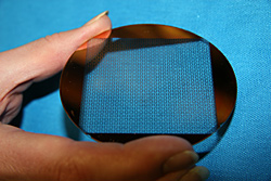
Firefighters watch as a fan, simulating wind, changes airflow and smoke conditions during experiments in a seven-story high-rise abandoned apartment building on New York City's Governors Island. The NIST tests examined firefighting techniques such as the use of positive pressure ventilation fans, wind control devices and hose streams to control or suppress heat and smoke from wind driven fires.
Credit: NIST
View hi-resolution image |
National Institute of Standards and Technology (NIST) fire protection engineers turned an abandoned New York City (NYC) brick high-rise into a seven-story fire laboratory last month to better understand the fast-moving spread of wind-driven flames, smoke and toxic gases through corridors and stairways of burning buildings. The experiments on NYC’s Governors Island, conducted in partnership with the Fire Department of New York (FDNY) and New York’s Polytechnic University, examined the effectiveness of firefighting tactics such as the use of positive pressure ventilation fans, wind control devices and hose streams to control or suppress deadly heat and smoke from the wind-driven fires.
Between 1985 and 2002, 1,600 civilians died and more than 20,000 people were injured in approximately 385,000 high-rise building fires in the United States, according to the National Fire Protection Association. Due to temperature differences between the outside and inside of a building on fire, open doors and broken windows far from the actual site of the fire can increase the movement of hot gases and smoke dramatically. Wind-driven flames, heat and smoke with temperatures exceeding 815 C (1500 F) can speed across entire floors and around corridors without warning. Smoke and heat entering stairwells often can block the evacuation of occupants and can hinder firefighting operations.
To develop an understanding of the wind-driven fires and measure the impact of the firefighting tactics, NIST researchers placed cameras, temperature and pressure sensors throughout the building. From a safe ground floor monitoring post, the researchers with laptops monitored the progress of intentionally set fires raging through the apartments and public corridors. They recorded, second-by-second, the effects of opening or closing doors and windows both near and far from the blaze.
Positive pressure ventilation fans, prototype wind control devices and prototype high-rise fire suppression nozzles, which were developed by FDNY, all had a positive impact on controlling the effects of a wind-driven fires.
Research findings from the Governors Island experiments are expected to help improve fire service guidelines for combating high-rise fires, enhance firefighter safety, fire ground operations and use of equipment. NIST expects to issue a report on the high-rise experiments by November 2008. The Department of Homeland Security’s (DHS) Federal Emergency Management Agency (FEMA) funded the Governors Island tests under its “Assistance to Firefighters” grant program.
For more information on NIST fire research in wind-driven fire research visit “Research Spotlight” at Fire.gov (www.fire.gov) and a recent NIST study reviewing six Positive Pressure Ventilation (PPV) experiments conducted in a Chicago high-rise building, “Evaluating Positive Pressure Ventilation in Large Structures: High Rise Fire Experiments” (2008). See also coverage here in “Fans Clear High-Rise Stairwells of Smoke” (2007) and “NIST Test Fans the Flames for High-Rise Fire Safety” (2006).
Media Contact: John Blair, john.blair@nist.gov, (301) 975-4261
NIST Team Proves Bridge from Conventional to Molecular Electronics Possible
 |
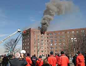
Side and top views of the NIST molecular resistor. Above are schematics showing a cross-section of the full device and a close-up view of the molecular monolayer attached to the CMOS-compatible silicon substrate. Below is a photomicrograph looking down on an assembled resistor indicating the location of the well.
Credit: NIST
View hi-resolution image |
Researchers at the National Institute of Standards and Technology (NIST) have set the stage for building the “evolutionary link” between the microelectronics of today built from semiconductor compounds and future generations of devices made largely from complex organic molecules. In an upcoming paper in the Journal of the American Chemical Society,* a NIST team demonstrates that a single layer of organic molecules can be assembled on the same sort of substrate used in conventional microchips.
The ability to use a silicon crystal substrate that is compatible with the industry-standard CMOS (complementary metal oxide semiconductor) manufacturing technology paves the way for hybrid CMOS-molecular device circuitry—the necessary precursor to a “beyond CMOS” totally molecular technology—to be fabricated in the near future.
Scientists classify crystal structures by the particular plane or “face” cutting through the crystal that is exposed. Most research to date on silicon substrates for molecular electronic devices has been done with a crystal orientation that is convenient for organic molecules but incompatible with CMOS technologies. For their electronic device, the NIST team first demonstrated that a good quality monolayer of organic molecules could be assembled on the silicon orientation common to industrial CMOS fabrication, verifying this with extensive spectroscopic analysis.
They then went on to build a simple but working molecular electronic device—a resistor—using the same techniques. A single layer of simple chains of carbon atoms tethered on their ends with sulfur atoms were deposited in tiny 100-nanometer deep wells on the silicon substrate and capped with a layer of silver to form the top electrical contact. The use of silver is a departure from other molecular electronic studies where gold or aluminum has been used. Unlike the latter two elements, silver does not displace the monolayer or impede its ability to function.
The NIST team fabricated two molecular electronic devices, each with a different length of carbon chain populating the monolayer. Both devices successfully resisted electrical flow with the one possessing longer chains having the greater resistance as expected. A control device lacking the monolayer showed less resistance, proving that the other two units did function as nonlinear resistors.
The next step, the team reports, is to fabricate a CMOS-molecular hybrid circuit to show that molecular electronic components can work in harmony with current microelectronics technologies.
This work was funded in part by the NIST Office of Microelectronics Programs and the Defense Advanced Research Projects Agency (DARPA) MoleApps Program.
* N. Gergel-Hackett, C.D. Zangmeister, C.A. Hacker, L.J. Richter and C.A. Richter. Demonstration of molecular assembly on Si (100) for CMOS-compatible molecular-based electronic devices. Journal of the American Chemical Society, Vol. 130, No. 13 (April 2, 2008), pp 4259-4261. Published online March 7, 2008.
Media Contact: Michael E. Newman, michael.newman@nist.gov, (301) 975-3025
Loopy Photons Clarify ’Spookiness‘ of Quantum Physics
Researchers at the National Institute of Standards and Technology (NIST) and the Joint Quantum Institute (NIST/University of Maryland) have developed a new method for creating pairs of entangled photons, particles of light whose properties are interlinked in a very unusual way dictated by the rules of quantum physics. The researchers used the photons to test fundamental concepts in quantum theory.
In the experiment, the researchers send a pulse of light into both ends of a twisted loop of optical fiber. Pairs of photons of the same color traveling in either direction will, every so often, interact in a process known as “four-wave mixing,” converting into two new, entangled photons, one that is redder and the other that is bluer than the originals.
Although the fiber’s twist means that pairs emerging from one end are vertically polarized (having electric fields that vibrate up and down) while pairs from the other end are horizontally polarized (vibrating side to side), the setup makes it impossible to determine which path the newly created photon pairs took. Since the paths are indistinguishable, the weird rules of quantum physics say that the photon pairs actually will be in both states—horizontal and vertical polarization—at the same time. Until someone measures one, at which time both photons must chose one specific, and identical, state.
This “spooky action at a distance” is what caused Einstein to consider quantum mechanics to be incomplete, prompting debate for the past 73 years over the concepts of “locality” and “realism.” Decades of experiments have demonstrated that measurements on pairs of entangled particles don’t agree with the predictions made by “local realism,” the concept that processes occurring at one place have no immediate effect on processes at another place (locality) and that the particles have definite, preexisting properties (called “hidden variables”) even without being measured (realism).
Experiments so far have ruled out locality and realism as a combination. But could a theory assuming only one of them be correct? Nonlocal hidden variables (NLHV) theories would allow for the possibility of hidden variables but would concede nonlocality, the idea that a measurement on a particle at one location may have an immediate effect on a particle at a separate location.
Measuring the polarizations of the pairs of entangled particles in their setup, the researchers showed that the results did not agree with the predictions of certain NLHV theories but did agree with the predictions of quantum mechanics. In this way, they were able to rule out certain NLHV theories. Their results agree with other groups that have performed similar experiments.
* J. Fan, M.D. Eisaman and A. Migdall, Bright phase-stable broadband fiber-based source of polarization-entangled photon pairs. Physical Review A 76, 043836 (2007). Abstract at http://link.aps.org/abstract/PRA/v76/e043836.
** M.D. Eisaman, E.A. Goldschmidt, J. Chen, J. Fan and A. Migdall. Experimental test of non-local realism using a fiber-based source of polarization-entangled photon pairs. Physical Review A., upcoming.
Media Contact: Ben Stein, bstein@nist.gov, (301) 975-3097
NIST ‘Quantum Logic Clock’ Rivals Mercury Ion as World’s Most Accurate Clock
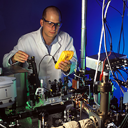 |
NIST physicist Till Rosenband adjusts the quantum logic clock, which derives its “ticks” from the natural vibrations of an aluminum ion (electrically charged atom). The aluminum ion is trapped together with one beryllium ion inside the copper-colored chamber in the foreground.
Credit: Copyright Geoffrey Wheeler
To receive a high-resolution version of this image please contact inquiries@nist.gov. |
An atomic clock that uses an aluminum atom to apply the logic of computers to the peculiarities of the quantum world now rivals the world’s most accurate clock, based on a single mercury atom. Both clocks are at least 10 times more accurate than the current U.S. time standard.
The measurements, described in a new paper,* were made in a yearlong comparison of the two next-generation clocks, both designed and built at the National Institute of Standards and Technology (NIST). The clocks were compared with record precision, allowing scientists to measure the relative frequencies of the two clocks to 17 digits—the most accurate measurement of this type ever made. The comparison produced the most precise results yet in the worldwide quest to determine whether some of the fundamental constants that describe the universe are changing slightly over time, a hot research question that may alter basic models of the cosmos.
The aluminum and mercury clocks are both based on natural atomic vibrations and would neither gain nor lose one second in over 1 billion years—if they could run for such a long time—compared to about 80 million years for NIST-F1, the U.S. time standard based on cesium atoms.
The mercury clock, first demonstrated in 2000, continues its reign as the world’s most accurate for now, by a margin of 20 percent over the aluminum clock, but the designers say both experimental clocks could be improved further. The aluminum clock has an advantage in being relatively insensitive to background magnetic and electric fields and temperature. It has the lowest known sensitivity of any atomic clock to temperature.
Both the clocks are based on ions vibrating at optical frequencies, which are 100,000 times higher than microwave frequencies used in NIST-F1 and other similar time standards. Because optical clocks divide time into smaller units, they can be far more precise. Highly accurate clocks are used to synchronize telecommunications networks and deep-space communications, and for satellite navigation and positioning. Next-generation clocks may also lead to new types of gravity sensors, which have potential applications in exploration for underground natural resources and fundamental studies of the Earth.
The new paper provides the first published evaluation of the operational quantum logic clock, so-named because it is a spin-off of NIST research on quantum computers. The NIST quantum logic clock uses two different kinds of ions, aluminum and beryllium, confined closely together in an electromagnetic trap and slowed by lasers to nearly “absolute zero” temperatures. Aluminum is a stable source of clock ticks, but its properties cannot be detected easily with lasers. The NIST scientists applied quantum computing methods to share information from the aluminum ion with the beryllium ion, so they could detect the aluminum clock’s ticks by observing light signals from the beryllium ion.
The work was supported in part by the Office of Naval Research and Disruptive Technology Office. For more details, photos and video, see “NIST ‘Quantum Logic Clock’ Rivals Mercury Ion as World’s Most Accurate Clock”
* T. Rosenband, D.B. Hume, P.O. Schmidt, C.W. Chou, A. Brusch, L. Lorini, W.H. Oskay, R.E. Drullinger, T.M. Fortier, J.E. Stalnaker, S.A. Diddams, W.C. Swann, N.R. Newbury, W.M. Itano, D.J. Wineland and J.C. Bergquist. Frequency ratio of Al+ and Hg+ single-ion optical clocks; metrology at the 17th decimal place. Science Express. Published online March 6, 2008.
Media Contact: Laura Ost, laura.ost@nist.gov, (303) 497-4880
Joint Research: Probing the Mysteries of a Surprisingly Tough Hydrogel
Some 46 million people suffer from arthritis in the United States alone. The worst cases require painful surgeries to drill holes in and reinforce joints. Now researchers working at the National Institute of Standards and Technology (NIST) are studying an unusually pliant yet strong synthetic cartilage replacement in hopes of providing arthritis victims with some relief. In a paper* presented at the March Meeting of the American Physical Society, NIST scientists and colleagues from Hokkaido University in Japan, reported on a gel that, while having the pliancy of gelatin, won’t break apart even when deformed over 1,000 percent. By using NIST’s neutron research facility to show how the molecules in the gel sustain such large deformations, the research team hopes to make it easier to design materials with even better mechanical properties.
Known as double-network hydrogels, the incredible strength of these new materials was a happy surprise when first discovered by researchers at Hokkaido in 2003. Most conventionally prepared hydrogels—materials that are 80 to 90 percent water held in a polymer network—easily break apart like a gelatin. The Japanese team serendipitously discovered that the addition of a second polymer to the gel made them so tough that they rivaled cartilage—tissue which can withstand the abuse of hundreds of pounds of pressure. A combination of a brittle hydrogel and a soft polymer solution leads to a surprisingly tough material.
Initial work using NIST’s neutron scattering techniques to explore the structure of the gel found unexpected results. The two polymers** were attracted to each other—despite the fact that one polymer is negatively charged and the other neutral—and can withstand a certain force before they can be pulled apart. The total amount of force that can be endured by this polymer pair gets amplified enormously because there are many contacts along each long chain. Efficacy of stress transfer between the long added chain and gel network forms the cornerstone of the toughening mechanism in DN-gels.
The latest paper discusses a proposed molecular-level toughening mechanism based on neutron scattering measurements that gather, in detail, how the two polymers behave when the gel is deformed. Under deformation, these two polymers arrange themselves into an alternating, well-ordered, periodic pattern that is repeated approximately every 2 microns. This periodic structure is 100 times larger than what is usually seen in molecules under deformation, and its formation elegantly dissipates a large amount of deformation energy to stabilize the gel and keep it from crumbling apart.
Establishing the details of the molecular structure will allow for more precise design of the next generation of hydrogels that are tough and rigid at the same time. Real cartilage goes through a process of constant daily destruction and regeneration under everyday stresses; the researchers hope a good synthetic cartilage could endure year after year under the rigors of the body before needing to be replaced.
* W.L. Wu, V.R. Tirumala, T. Tominaga, S. Lee, P. Butler, E.K. Lin, J.P. Gong and H. Furukawa. A molecular model for toughening in double-network hydrogels. Presented at the March Meeting of the American Physical Society, March 11, 2008, New Orleans, La. Session: J25.00006.
** The materials is made by adding polyacrylamide (PAAm) to a gel based on poly(2-acrylamide,2-methyl,1-propanesulfonicacid) (PAMPS).
Media Contact: Michael Baum, michael.baum@nist.gov, (301) 975-2763
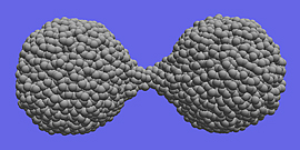
Nanomaterials Show Unexpected Strength Under Stress
 |
NIST researchers have shown that substances such as silica that are brittle in bulk exhibit ductile behavior at the nanoscale. Computer simulations demonstrate the material extension and necking that occurs during the separation of amorphous (top) and crystalline (bottom) silica nanoparticles.
Credit: NIST
View hi-resolution image of top image
View hi-resolution image of bottom image |
In yet another twist on the strangeness of the nanoworld, researchers at the National Institute of Standards and Technology (NIST) and the University of Maryland-College Park have discovered that materials such as silica that are quite brittle in bulk form behave as ductile as gold at the nanoscale. Their results may affect the design of future nanomachines.
NIST scientists Pradeep Namboodiri and Doo-In Kim and colleagues first demonstrated* the latest incongruity between the macro- and microworlds this past fall with direct experimental evidence for nanoscale ductility. In a new paper** presented at the March Meeting of the American Physical Society, NIST researchers Takumi Hawa and Michael Zachariah and guest researcher Brian Henz shared the insights they gained into the phenomenon through their computer simulations of nanoparticle aggregates.
At the macroscale, the point at which a material will fail or break depends on its ability to maintain its shape when stressed. The atoms of ductile substances are able to shuffle around and remain cohesive for much longer than their brittle cousins, which contain faint structural flaws that act as failure points under stress.
At the nanoscale, these structural flaws do not exist, and hence the materials are nearly “perfect.” In addition, these objects are so small that most of the atoms that comprise them reside on the surface. According to Namboodiri and Kim, the properties of the surface atoms, which are more mobile because they are not bounded on all sides, dominate at the nanoscale. This dominance gives an otherwise brittle material such as silica its counterintuitive fracture characteristics.
“The terms ‘brittle’ and ‘ductile’ are macroscopic terminology,” Kim says. “It seems that these terms don’t apply at the nanoscale.”
Using an atomic force microscope (AFM), Kim and Namboodiri were able to look more closely at interfacial fracture than had been done before at the nanoscale. They found that the silica will stretch as much as gold or silver and will continue to deform beyond the point that would be predicted using its bulk-scale properties.
Hawa, Henz and Zachariah’s simulations reaffirmed their study and added some additional details. They showed that both nanoparticle size and morphology—whether the material is basically crystalline or amorphous, for example—have an effect on the observed ductility and tensile strength because those factors influence the mobility of surface atoms. In the simulations, the smaller the particles in the aggregate the more ductile the material behaved. Crystalline structures exhibited greater strength when stressed and deformed long after the critical yield point observed macroscopically.
Namboodiri explained that although the work is very basic, these findings might one day inform the design of microelectronic mechanical devices.
* N. Pradeep, D-I. Kim, J. Grobelny, T. Hawa, B. Henz, and M. R. Zachariah. Ductility at the nanoscale: Deformation and fracture of adhesive contacts using atomic force microscopy. Applied Physics Letters, published online 15 November 2007.
** T. Hawa, B. Henz, and M. Zachariah. Computer simulations of nanoparticle aggregate fracture. Presented Wednesday, March 12, 2008, at the 2008 APS meeting in New Orleans, La.
Media Contact: Mark Esser, mark.esser@nist.gov, (301) 975-2767
Stunt Doubles: Ultracold Atoms Could Replicate the Electron ‘Jitterbug’
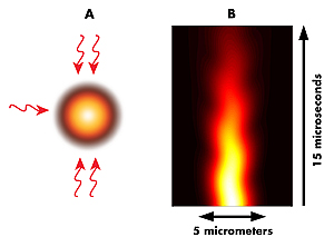 |
A) Optical lattice of five laser beams trapping an atomic cloud. Color scale indicates cloud density: black is low, white high. B) Jittering motion of the atomic cloud in the optical lattice. The horizontal axis represents the spatial distribution of the cloud along one direction, while the vertical axis shows the variation of cloud density with time.
Credit: NIST
View hi-resolution image |
Ultracold atoms moving through a carefully designed arrangement of laser beams will jiggle slightly as they go, two NIST scientists have predicted.* If observed, this never-before-seen “jitterbug” motion would shed light on a little-known oddity of quantum mechanics arising from Paul Dirac’s 80-year-old theory of the electron.
Dirac’s theory, which successfully married the principles of Einstein’s relativity to the quantum property of electrons known as spin, famously predicted that the electron must have an antiparticle, subsequently discovered and named the positron. More enigmatically, the Dirac theory indicates that an isolated electron moving through empty space will vibrate back and forth. But this shaking—named Zitterbewegung from the German for ‘trembling motion’—is so rapid and so tiny in amplitude that it has never been directly observed.
Jay Vaishnav and Charles Clark of the Joint Quantum Institute, a partnership of NIST and the University of Maryland, have devised an experimental arrangement in which atoms are made to precisely mimic the behavior of electrons in Dirac’s theory. The atoms will show Zitterbewegung—but with vibrations that are slow enough and large enough to be detected.
Vaishnav and Clark’s proposal begins with an atom—rubidium-87 is an example—that has a ‘tripod’ arrangement of electron energy levels, consisting of one higher energy level above three equal-energy lower levels. Suppose, say the researchers, that such atoms are placed in a region crisscrossed by lasers at specific frequencies. Two pairs of laser beams face each other, creating a pattern of standing waves, while a third laser beam is set perpendicular to the other two.
Given the proper frequencies of light, a perfectly stationary “tripod” atom at the intersection will have the energy of its upper state and one of the three lower states slightly changed. To a moving atom, however, the electromagnetic field will look a little different, and in that case the energies of the other two lower states also change slightly.
Remarkably, those two states, moving in this particular arrangement of laser light, are governed by an equation that’s exactly analogous to the Dirac equation for the two spin states of an electron moving in empty space. In particular, as the atom moves it flips back and forth between the two states, and that flipping is accompanied by a jiggling back and forth of the atom’s position—a version of Zitterbewegung with a frequency measured in megahertz, 100 trillion times slower than the vibration of a free electron.
Other arrangements of lasers and atoms have been used to cleanly simulate a variety of quantum systems, says Vaishnav. Examples includes recent studies of the mechanisms of quantum magnetism and high-temperature superconductivity.** What’s unusual about this new proposal, she adds, is that it offers a simulation of a fundamental elementary particle in free space and may offer access to an aspect of electron behavior that would otherwise remain beyond observational scrutiny.
* J.Y. Vaishnav and C.W. Clark. Observation of zitterbewegung in ultracold atoms. Presented at the March Meeting of the American Physical Society, March 10, 2008, New Orleans, La., Session A14.00003.
** I. Bloch. Towards quantum magnetism with ultracold quantum gases in optical lattices. Presented at the March Meeting of the American Physical Society, March 12, 2008, New Orleans, La., Session P7.00003. and A.M. Rey. Probing and controlling quantum magnetism with ultra-cold atoms. Presented at the March Meeting of the American Physical Society, March 12, 2008, New Orleans, La., Session P7.00004.
Media Contact: Ben Stein, bstein@nist.gov, (301) 975-3097
Copolymers Block Out New Approaches to Microelectronics at NIST
 |
A novel technique for controlling the orientation of nanostructures (red and blue) is to use disordered, roughened substrates. Silica nanoparticles (orange), cast onto silicon substrates (grey), create ‘tunable’ substrates that can control self-assembly, despite inherent disorder.
Credit: NIST
View hi-resolution image |
In response to the electronics industry’s rallying cry of “smaller and faster,” the next breakthroughs in the electronics size barrier are likely to come from microchips and data storage devices created out of novel materials such as organic molecules and polymers. With innovative measurement techniques and new ways to position the molecules, NIST researchers reported at the March Meeting of the American Physical Society how they have improved manipulation of so-called block copolymers—polymers made of a mixture of two or more different molecule building blocks that are tethered at a junction point—which can form arrays of tiny dots that could be used as the basis for electronic components that pack terabytes (1000 gigabytes) of memory in something as small as a pack of gum.
One of the challenges in polymer nanotechnology is how to control their self-assembly—a hard-to-control process for materials that require precision. An important recent NIST accomplishment has been in developing accurate measurements of thin film polymeric nanostructure in 3-D. (Ironically, while determining atomic structure is well-established, measuring the slightly larger internal structure of the polymers—on the order of 10 to 20 nanometers—is much harder.) Ron Jones, together with colleagues from NIST, the University of Maryland and IBM, has used NIST’s neutron scattering and reflectivity facility to deflect neutrons off block copolymer films from many different angles. By combining the many 2-D neutron scattering pictures into a single composite scattering pattern, this technique provides the first quantitative method for imaging the 3-D internal structure of thin film polymeric nanostructures using neutron scattering—a crucial tool to see if the nanoscale polymer structures are in their required positions.1
NIST researchers also have developed new insights on how best to nudge these self-assembling materials into those positions. August Bosse will report on computer simulations that model how the polymers assemble when they are placed on templates lined with troughs separated by crests.2 When a heated zone is swept across the template, the polymer molecules assemble into almost defect-free, well-aligned lines faster over the entire template, an important feature for nanotech manufacturing applications.3 Sangcheol Kim (working with a team that included researchers from the University of Maryland and IBM) has found that changing the surface chemistry of the template by making some parts hydrophillic and some parts hydrophobic also can elegantly control the dimension of the block-copolymer pattern relative to the chemical template.4
And last, with all this emphasis on precise placement, NIST researcher Kevin Yager, has learned that sometimes sloppier is better. By purposely roughening up his templates with a sprinkling of chemically modified nanoparticle silica, he has forced block copolymers into standing perpendicular to the template—a feat that is generally considered tough to manage but important for nanotech applications.5 Of course, the inner structure of the polymers are not orderly with this technique, but for those applications where only the surface needs to be smooth, this is an ideal, inexpensive way to achieve vertical structures.
1 R. Jones, X. Zhang, S. Kim, A. Karim, R. Briber and H. Kim. Orientation distribution for thin film block copolymers. Presented at the March Meeting of the American Physical Society, March 12, 2008, New Orleans, La. Session: Q22.00007.
2 A. Bosse, R. Jones and A. Karim. Fluctuation-induced line-edge roughness in nano-confined block copolymer thin films. Presented at the March Meeting of the American Physical Society, March 11, 2008, New Orleans, La. Session: L22.00010.
3 A. Karim. INVITED TALK. Templated Self-Assembly of Block Copolymer Thin Films. Presented at the March Meeting of the American Physical Society, March 10, 2008, New Orleans, La. Session: B4.00002.
4 S. Kim, H-J. Lee, R.L. Jones, A. Karim, R.M. Briber and H-C. Kim. Precise control of 3-dimensional block copolymer assembly using 2-dimensional chemical templates. Presented at the March Meeting of the American Physical Society, March 10, 2008, New Orleans, La. Session: A25.00010.
5 K. Yager, A. Karim and E. Amis. Disordered nanoparticle interfaces for defect-tolerance in the self-assembly of block-copolymers. Presented at the March Meeting of the American Physical Society, March 12, 2008, New Orleans, La. Session: P18.00001.
Media Contact: Michael Baum, michael.baum@nist.gov, (301) 975-2763
New NIST Detector Can ‘See’ Single Neutrons Over Broad Range
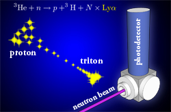 |
Neutron absorption by 3He yields tens of Lyman alpha photons, which result from the most fundamental energy jump in the hydrogen atom. This schematic illustrates the operation of a prototype Lyman alpha neutron detector (LAND).
Credit: NIST
View hi-resolution image |
Researchers at the National Institute of Standards and Technology (NIST) and the University of Maryland have developed a new optical method that can detect individual neutrons and record them over a range of intensities at least 100 times greater than existing detectors. The new detector, described at the March Meeting of the American Physical Society* by Charles Clark, a Fellow of the Joint Quantum Institute of NIST and the University of Maryland, promises to improve existing neutron measurements and enable tests of new phenomena beyond the Standard Model, the basic framework of particle physics.
The prototype laboratory device is based on a process first observed by the research team: the emission of light from hydrogen atoms produced when neutrons are absorbed by helium-3 atoms (3He). Lyman alpha light, discovered by Harvard physicist Theodore Lyman in 1906, results from the jump between the two lowest-energy states of the hydrogen atom. Although it is the brightest light emitted by the sun and is one of the most abundant forms of light in the universe, Lyman alpha is invisible to the eye because it lies in the far ultraviolet region of the optical spectrum. It is strongly absorbed by most substances and can travel through only about a millimeter of air.
Helium gas, however, does not absorb Lyman alpha light. When a neutron is absorbed by a helium-3 atom, one atom of hydrogen and one atom of tritium (a heavy form of hydrogen) are produced. These atoms fly apart at high speeds, can be excited by collisions with surrounding helium gas, and subsequently emit Lyman alpha light. This light is recorded by the new device, known as the Lyman alpha neutron detector (LAND).
Using an ultracold neutron beam at the NIST Center for Neutron Research, the research team has discovered that Lyman alpha light is generated with surprisingly high efficiency: about 40 photons are generated per neutron for helium gas at atmospheric pressure. According to Alan Thompson, neutron expert on the team, “This device thus has the potential to detect both single neutrons and large numbers of neutrons, which is very difficult to do with present neutron detectors based on electrical discharges.”
The use of an optical means of detection, rather than an electronic one, also offers the prospect of at least a hundredfold improvement in neutron detectors’ dynamic range (the spread in recordable neutron intensity from faint to bright). This stems from the fact that optical detectors respond more quickly than electronic detectors, which suffer from longer periods of inactivity known as “dead time.”
With further development, this new method can potentially lead to better measurements at existing neutron facilities (for example, neutron diffraction instruments at the NIST Center for Neutron Research) and enable new tests of physics beyond the Standard Model. Measurements at NIST of a property in neutrons known as the electric dipole moment and more precise measurements of the neutron lifetime are planned.
* C. W. Clark, A. K. Thompson, M .A. Coplan, J. W. Cooper, P. Hughes and R. E. Vest, Observation of the n(3He,t)p reaction by detection of far-ultraviolet radiation. Presented at the 2008 March Meeting of the American Physical Society, New Orleans, La., March 10-14, 2008. paper B14.00010.
Media Contact: Ben Stein, bstein@nist.gov, (301) 975-3097
All Done With Mirrors: NIST Microscope Tracks Nanoparticles in 3-D
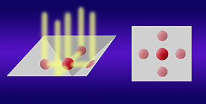 |
Heart of the orthogonal tracking microscope system developed at NIST is this nanoparticle solution sample well etched in silicon. Careful orientation of the silicon crystal makes it possible to chemically etch angled sides in the well so smooth they act as mirrors. In this configuration, four side views of a nanoparticle floating in solution (left) are reflected up. A microscope above the well sees the real particle (center, right) and four reflections that show the particle's vertical position.
Credit: Talbott/NIST
View hi-resolution image |
Click here for AVI movie clip
Credit: NIST |
Video of a fluorescent polystyrene sphere 190nm in diameter captured with the NIST orthogonal tracking microscope. The view is of an upper-left corner of the sample well. The glowing ball at the bottom right of the image is the particle, the other two moving glows are reflections.
|
AVI clips require Windows Media Player (or equivalent), a free download – click here. |
A clever new microscope design allows nanotechnology researchers at the National Institute of Standards and Technology (NIST) to track the motions of nanoparticles in solution as they dart around in three dimensions. The researchers hope the technology, which NIST plans to patent, will lead to a better understanding of the dynamics of nanoparticles in fluids and, ultimately, process control techniques to optimize the assembly of nanotech devices.
While some nanoscale fabrication techniques borrow from the lithography and solid state methods of the microelectronics industry, an equally promising approach relies on “directed self-assembly.” This capitalizes on physical properties and chemical affinities of nanoparticles in solutions to induce them to gather and arrange themselves in desired structures at desired locations. Potential products include extraordinarily sensitive chemical and biological sensor arrays, and new medical and diagnostic materials based on “quantum dots” and other nanoscale materials. But when your product is too small to be seen, monitoring the assembly process is difficult.
Microscopes can help, but a microscope sees a three-dimensional fluid volume as a 2-D plane. There’s no real sense of the “up and down” movement of particles in its field of view except that they get more or less fuzzy as they move across the plane where the instrument is in focus. To date, attempts to provide a 3-D view of the movements of nanoparticles in solution largely have relied on that fuzziness. Optics theory and mathematics can estimate how far a particle is above or below the focal plane based on diffraction patterns in the fuzziness. The math, however, is extremely difficult and time consuming and the algorithms are imprecise in practice.
One alternative, NIST researchers reported at the annual March Meeting of the American Physical Society,* is to use geometry instead of algebra. Specifically, angled side walls of the microscopic sample well act as mirrors to reflect side views of the volume up to the microscope at the same time as the top view. (The typical sample well is 20 microns square and 15 microns deep.) The microscope sees each particle twice, one image in the horizontal plane and one in the vertical. Because the two planes have one dimension in common, it’s a simple calculation to correlate the two and figure out each particle’s 3-D path. “Basically, we reduce the problem of tracking in 3-D to the problem of tracking in 2-D twice,” explains lead author Matthew McMahon.
The 2-D problem is simpler to solve—several software techniques can calculate and track 2-D position to better than 10 nanometers. Measuring the nanoparticle motion at that fine scale—speeds, diffusion and the like—will allow researchers to calculate the forces acting on the particles and better understand the basic rules of interaction between the various components. That in turn will allow better design and control of nanoparticle assembly processes.
* M. McMahon, A. Berglund, P. Carmichael, J. McClelland and J.A. Liddle. Orthogonal tracking microscopy for nanofabrication research. Presented at the 2008 March Meeting of the American Physical Society, New Orleans, La., March 10-14, 2008.
Media Contact: Michael Baum, michael.baum@nist.gov, (301) 975-2763
NIST Seeks Public Comment on New Technology Innovation Program Regulations
The Commerce Department’s National Institute of Standards and Technology (NIST) is seeking public comments on its proposed regulations (rule) for operating the Technology Innovation Program (TIP) created as part of the America COMPETES Act passed in August. The proposed rule describing evaluation and award criteria and other specifics of the new competitive funding program was published in the Federal Register on March 7, 2008.
TIP was established “to support, promote, and accelerate innovation in the United States through high-risk, high-reward research in areas of critical national need.” The proposed rule covers research grants and/or cooperative agreements to single small- or medium-sized businesses and joint ventures. “High-risk, high-reward research” is defined as research that has the potential for yielding transformational results with far-ranging or wide-ranging implications; addresses areas of critical national need that support, promote, and accelerate innovation in the United States and is within NIST’s areas of technical competence; and is too novel or spans too diverse a range of disciplines to fare well in the traditional peer-review process for grants.
TIP awards will be cost-shared and made on the basis of merit competitions, as detailed in the proposed rule. Single, for-profit, companies or joint ventures made up of companies, institutions of higher education, nonprofit research institutes and/or government laboratories other than NIST are eligible for TIP support, with some restrictions on the size of companies, ownership and the types of research. TIP awards will be limited to no more than $3 million total over three years for a single-company project and no more than $9 million total over five years for a joint venture. Other operational features of the TIP, including the handling of intellectual property rights, reporting and auditing requirements and performance monitoring and evaluation, also are detailed in the proposed rule.
TIP plans to conduct an FY 2008 competition after publication of the final rule.
Comments on the proposed rule must be submitted by April 21, 2008. The proposed rule* and additional information are available on the TIP Web site www.nist.gov/tip.
To read the legislation authorizing TIP, see “P.L.110-69, Sec. 3012 Technology Innovation Program” (requires Acrobat Reader, a free download.)
* Docket No. 071106659-7661-01, “Technology Innovation Program”. Federal Register V. 73, Num. 46, March 7, 2008, p.12305
Media Contact: Michael Baum, michael.baum@nist.gov, (301) 975-2763
NIST Votes for U.S. Approval of the Modified Office Open XML Standard
The Commerce Department’s National Institute of Standards and Technology (NIST) has voted for U.S. approval of a modified version of the proposed international standard known as Office Open XML (OOXML). NIST is one of 17 voting members of the U.S. body known as the InterNational Committee for Information Technology Standards Executive Board (INCITS EB). This NIST vote comes in response to modifications made to OOXML at an international meeting last month.
Last summer, the U.S. body initially voted on a ballot from the international standards organization ISO/IEC that would fast-track OOXML to the status of an international standard. The U.S. body voted “approve, with comments” on the ballot, but the proposed standard failed to win approval in the initial international tally.
In late February, comments from national bodies were considered at an ISO/IEC ballot resolution meeting in Geneva, Switzerland. Participants in the ballot resolution meeting modified the proposed OOXML standard in response to comments from the national bodies. Based upon the changes to the OOXML standard agreed to at the ballot resolution meeting, national bodies have until March 29, 2008, to reconsider their original votes.
The U.S. body has voted to approve the modified OOXML standard with 11 members, including NIST, voting “yes,” four members voting “no,” one member voting to abstain and one member not casting a vote. If the final international vote tally is sufficient for approval, OOXML will be published as an ISO/IEC international standard. If the final vote fails, then OOXML could still be submitted for consideration again to an ISO/IEC subcommittee known as JTC 1/SC 34.
If approved, OOXML would join the Open Document Format (ODF) as another worldwide standard for “open documents.” Open document standards are applicable to word processing, spreadsheets and other types of documents intended to allow computer users to exchange documents more easily between software programs and across hardware platforms. Presently, most office application software relies on proprietary file formats. OOXML is intended to enable users to read and write files in an open document format that Microsoft and other OOXML proponents have stated will be free of any proprietary content.
Additional information:
Links to earlier news releases on NIST and OOXML:
Media Contact: Ben Stein, bstein@nist.gov, (301) 975-3097
Quick Links
NIST Acting Director Turner Testifies on FY 2009 Budget Request
On March 11, National Institute of Standards and Technology (NIST) Acting Director James Turner testified before the committees of the Senate and House on the President’s proposed FY 2009 budget.
Turner’s testimony to the Senate Commerce, Science and Transportation Subcommittee on Science, Technology and Innovation was on the proposed fiscal 2009 budget for basic U.S. research in science and technology, including the budgets for the National Institute of Standards and Technology and the National Science Foundation, as well as interagency science programs addressing climate change, nanotechnology and information technology.
His testimony before the House Science and Technology Subcommittee on Technology and Innovation concerned NIST’s FY 2009 budget request and was titled “What are the Right Technology Investments to Promote U.S. Innovation and Competitiveness?”
Copies of Turner’s prepared states are available from NIST’s Office of Congressional and Legislative Affairs.
James W. Serum, president of SciTek Ventures and chair of the NIST Visiting Committee on Advanced Technology (VCAT), the agency’s primary private-sector advisory group, also testified before before the House committee on NIST's budget request. Serum's prepared testimony is available on the VCAT Web site, www.nist.gov/director/vcat/.
NIST Advisory Committee Issues 2007 Annual Report
The Visiting Committee on Advanced Technology (VCAT) of the National Institute of Standards and Technology (NIST), the agency's primary private-sector advisory group, has sent its 2007 Annual Report to the Congress.
The VCAT was established by Congress in 1988 to review and make recommendations on NIST’s policies, organization, budget and programs. The 2007 report includes detailed analyses by special subcommittees of the VCAT on NIST's role and activities in the areas of bioscience and healthcare, nanotechnology and information technology, with specific recommendations on future research directions. The report also expresses the committee's strong support for the significant program increases in the FY 2009 President's budget request for NIST as part of the American Competitiveness Initiative (ACI) and the America COMPETES Act.
For the full text of the VCAT report, see “2007 Annual Report, Visiting Committee on Advanced Technology of the National Institute of Standards and Technology” (requires Acrobat Reader, a free download.)
The next NIST VCAT meeting will be held on June 10-11 in Gaithersburg, Md.. VCAT meetings are open to the public. For more information, see www.nist.gov/director/vcat/.
Report Identifies Three Key R&D Priorities for Future Manufacturing
A new report identifies and describes research and development priorities for the future of three critical, high-tech U.S. manufacturing areas—hydrogen energy technologies, nanomanufacturing and intelligent and integrated manufacturing. The report, Manufacturing the Future: Federal Priorities for Manufacturing R&D, was prepared by the Interagency Working Group (IWG) on Manufacturing R&D of the National Science and Technology Council’s (NSTC) Committee on Technology.
Competing successfully in today’s fast-paced global community requires rapid innovation, research and production methods to cost-effectively bring products to market. The report describes the significance of each of the three critical manufacturing R&D areas, details the challenges essential for progress, discusses existing interagency collaborations and provides recommendations for future research. It identifies these areas as potentially leveraging scientific and technological advances to transform knowledge and materials into valuable products.
Much of this research falls under the American Competitiveness Initiative, a government-funded mandate to increase investments in R&D, education and entrepreneurship. These manufacturing areas also correspond to existing priorities established by the federal government through the President’s Hydrogen Fuel Initiative, the National Nanotechnology Initiative and the Networking and Information Technology Research and Development Program. For more details, see “Report Identifies Three Key R&D Priorities for Future Manufacturing”.
Web Site Offers Easy Access to Life-Saving Fire Service Research
A new National Institute of Standards and Technology (NIST) Web site offers easy access to reports of NIST fire investigations, summaries of research projects and videos of NIST fire research experiments and tests. The site Fire.gov, builds on the success of the NIST electronic quarterly of the same name that reports on fire research activities around the world.
NIST fire engineers created Fire.gov to provide ready access to their efforts to develop and apply technology, measurements and standards to better understand the behavior, prevention and control of fires and to improve firefighting operations and equipment, fire suppression, fire investigations and disaster response.
Firefighters can easily find NIST research on methods and technologies for fighting fires, including safe use limits for turnout gear, the performance of thermal imaging cameras, Personal Alert Safety System (PASS) devices, Positive Pressure Ventilation (PPV) techniques and the impact of firefighting hose stream methods. Current and past issues of the Fire.gov newsletter, sponsored by the United States Fire Administration (USFA), are still featured on the new site.
The site also links to NIST studies on flashover fires, structural collapses and specific disaster investigations, including the investigation of the 2003 Station Nightclub fire that claimed the lives of 100 people and an analysis of the 2003 Cook County Administration Building fire that killed six people and injured several more.
The new web page complements links to useful software tools, reports, and videos with links to a wide variety of private, professional and government fire organizations.
April Conferences Focus on Scanning Advances
Since the advent of the scanning electron microscope (SEM) in the 1930s, that instrument and its many and diverse descendents—including atomic force, scanning tunneling, confocal and helium ion microscopes—have unlocked microscopic worlds down to the atomic scale. “Scanning 2008,” a two-day conference on April 15-17, 2008, at the National Institute of Standards and Technology (NIST) in Gaithersburg, Md., will bring together microscopists, specializing in everything from scanned optics to scanned particle beams, to discuss current research and new advances in the field.
Conference topics will include forensic applications of SEM, scanning ion microscopy, quality assurance in SEM and micro characterization, silicon drift detectors, biological environmental/variable pressure SEM, modeling for critical SEM and microanalysis applications, scanning probe microscopy and scanning optical microscopy.
The meeting will feature tours of select NIST facilities, including a helium ion microscope, a high speed X-ray mapping facility using a silicon drift detector, a micro X-ray fluorescence X-ray spectrum imaging facility and others.
Registration for the conference closes April 8. To register or for more information, see the Scanning 2008 registration page. You also may view a preliminary program here.
|