
|
|||||||||
|
Technology at a Glance is a quarterly newsletter from the National Institute of Standards and Technology reporting on research results, funding programs, and manufacturing extension and technology services. If you have comments or general questions about this newsletter or if you would like to receive the four-page, color newsletter in hard copy, please email your mailing address to Gail Porter, editor, or call (301) 975-3392. About Technology at a Glance. [Technology at a Glance Search] [Technology at a Glance Archives] |
|||||||||
|
|
|||||||||
|
|

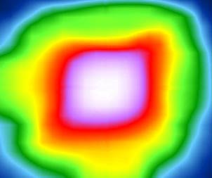 |
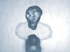
It will never
run in theaters, but this colorful movie has a cult following all
the same.
The “thermal contour” movie reveals what happens to a microhotplate, a NIST-developed technology that shows promise for a variety of gas-sensing applications, when it is heated and cooled. The devices are attractive for use in low-cost gas sensors, which might be used, for example, to detect freshness of food products or the leakage or presence of harmful chemicals.
The small size
and fast heating speed of these tiny, micromachined devices previously
made it difficult to measure dynamic temperature distribution, so
NIST researchers used a new high-speed transient thermal imaging system
(originally developed by NIST to study heating in power semiconductor
devices) to make the movies.
The imaging system
collects temperature information every microsecond for each 15 micrometer
square of space on the microhotplate. The system works by successively
acquiring temperature response as a function of time at each coordinate
of the device being tested, and by using a coordinate-translation
scheme to move between points. The thermal responses at different
points are reconstructed to make the thermal contour movie. The colors
in the graphic [above] indicate temperatures on a microhotplate surface
where white is the hottest and blue is the coolest.
Components include
an infrared microscope set up to “stare” at a 15 micrometer
region of the device being tested. A digitizing oscilloscope is used
for data acquisition. A temperature controller is used to maintain
the test device at a desired temperature and to facilitate calibration
of the emissions with a light chopper. A coordinate motion
controller is used to change coordinates on the device. And sophisticated
computer-controlled instrumentation with a high-level user interface
is used to make the high-speed thermal image measurements.
NIST researchers
found that the thermal imaging system can be used to optimize the
design of microhotplates, which consist of a heater, a metal thermometer/heat
distribution plate, and electrical contacts, all separated by insulating
layers.
Contact: Allen Hefner, (301) 975-2071.
![]()
Solar
Energy Home Runs on Ribbons
In a new twist
on the American dream, a “Zero-Energy Cottage” demonstrates
how a homeowner might do away with those pesky utility bills.
The 1,700-square-foot,
two-bedroom, two-bath house features a number of environmentally friendly
designs, materials, and systems, including solar electric panels made
by Evergreen Solar of Marlboro, Mass. The company developed an innovative
approach to making its technology with co-funding from NIST’s
Advanced Technology Program. Designed to generate as much energy as
it needs, the cottage is a project of the Captain Planet Foundation,
which supports environmental projects for kids.
Evergreen Solar
makes solar panels—which convert sunlight to electricity—using
a patented “String Ribbon” technique. Ultrathin crystalline
silicon is produced directly from molten silicon, a streamlined process
that avoids the waste and cost of slicing solid material blocks. String
Ribbon yields more than twice as many solar cells per pound of silicon
as typical methods, according to the company.
The three-year project overcame significant technical challenges,
including development of an active after-heater concept for precise
control of thermal gradients and stresses in the silicon as it is
formed and cools. Ribbon thickness was reduced from 300 micrometers
to less than 100 micro-meters, while the width was doubled to 8 centimeters.
These thinner, wider solar-grade ribbons also can be grown faster
with the after heater.
As a result of
the project, Evergreen Solar more than doubled furnace output and
attracted venture capital funding to build a new manufacturing plant.
The company has shipped more than 10,000 panels, which are used worldwide
for both grid-connected and remote power applications. They were used
in California to meet demand spurred by the recent energy crisis,
for example, and installed on Tokyo’s World Trade Center.
Contact: Rex D’Agostino, (508) 357-2221, Web site: www.evergreensolar.com.
![]()
Circuits
Sized Without Contact
A novel electrical
technique for measuring the widths (or critical dimensions) of features
patterned on the photomasks used in semiconductor manufacturing has
been developed by a NIST guest researcher from George Washington University
based on concepts originating at NIST. This technique—which can
provide measurements applicable to integrated circuits with 0.18-micrometer
lines, the state of the art—offers a potentially less expensive
alternative to conventional industrial metrology methods.
Test structures
are included in the designs patterned on photomasks so that suppliers
and users can measure parameters, such as width, of selected features.
The new technique measures the conduction characteristics of specific
features on the test structures,and their widths are derived from
this information. The relationship between electrical behavior and
size has long been used to determine linewidth; the innovation here
is that the electric signals are measured without physically contacting
the test structure, reducing the danger of damaging or contaminating
the mask.
An alternating-current
(AC) signal is delivered using a specially designed sensor located
in close proximity to, but not contacting, the test structure.
Analysis of this
AC signal provides a measure of the capacitance (a conductive device’s
capability to store electrical energy) between the sensor and the
test structure.
From this measurement,
the feature width is derived. Although the procedure appears straightforward,
turning this concept into a practical tool proved difficult.
The new test device
was fabricated by VTT in Finland with pioneering manufacturing methods.
A major achievement of the project was finding a way to reduce the
effects of “stray” capacitance and, thereby, improve the
signal-to-noise ratio.
Contact: Richard Allen, (301) 975-5026.
![]()
Ion
Beam Analyses Trace Quantities
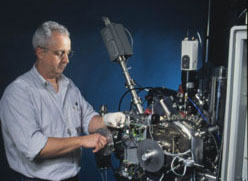 |
From semiconductor
chips to radioactive elements, a variety of materials and surfaces
are routinely characterized by secondary ion mass spectrometry (SIMS),
which offers high sensitivity, monolayer (single atom thickness) sampling
depth, and high spatial resolution. In SIMS, a surface is bombarded
in a vacuum with an energetic primary ion beam to produce characteristic
“secondary ion” signals that provide information on the
surface composition of the sample (ions are atoms possessing a net
electrical charge). NIST is a leader in the development and application
of SIMS, which is used for chemical analysis of the elemental and
molecular composition of a variety of industrially relevant materials,
including semiconductors, metals, polymers and pharmaceuticals.
Now, NIST
has a rare new SIMS instrument, one of only three of its type in the
United States, that offers superior sensitivity in detecting and distinguishing
among elements at trace levels with micrometer spatial resolution.
The new instrument (called an IMS 1270), offers very high secondary
ion transmission combined with high mass resolution and the
ability to simultaneously detect selected isotopes (isotopes are atomic
species of the same element with different masses). This capability
makes it especially useful for the precise measurement of isotope
ratios for elements at trace level concentrations. The room-sized
instrument is currently undergoing acceptance testing at NIST. Whereas
the two other IMS 1270s in this county are used primarily to characterize
geological materials, NIST scientists plan to apply their instrument
to a variety of basic research, standards, and industrial problems.
For instance,
the new instrument will be used to explore ultrahigh sensitivity measurements
of the abundance of dopant elements and metals in silicon wafers for
semiconductor manufacturing applications. Studies are planned to examine
the distribution of chemotherapeutic agents in tissue cell cultures
using molecules tagged with isotopic tracers. Other possible uses
include investigation of the need for standards and measurement methods
for geochemical applications, such as the analysis of samples from
energy exploration sites.
Contact: Albert Fahey, (301) 975-2185.
![]()
Getting
the Drop on Fire Quenchers
 |
 |
 |
 |
 |
 |
 |
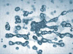 |
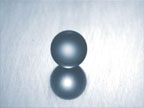
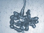
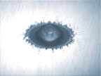
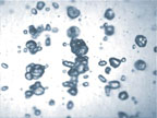
The behavior
of tiny droplets of new liquid fire suppressants may play a big role
in fire-fighting effectiveness. The new suppressants are proposed
to replace halon suppressants now being phased out because they cause
damage to stratospheric ozone.
The effectiveness
of a suppressant depends on many factors. Do the droplets evaporate
quickly or cling to a hot surface? Do they spread, shrink, splash,
or levitate? Liquid droplet interactions with surfaces have been studied
for more than 100 years, but the complicated fluid mechanics process
is still not well understood. Moreover, few studies have addressed
what happens to water droplets containing fire-suppressing additives.
NIST researchers
are studying the collision dynamics of single droplets, about 2.7
mm in diameter, as they strike a heated stainless steel surface. In
one set of experiments, the behavior of pure water was compared to
that of a solution with salt-containing additives (30 percent sodium
acetate trihydrate). The researchers recorded what happened to the
droplets at different impact energies and at different surface temperatures
using a high-speed digital camera.
Among the
findings, for both water (left column of photos) and additive-containing
droplets (right column), the disk-shaped liquid film formed on the
surface after impact grew in diameter at higher impact velocity, possibly
providing increased surface cooling. The presence of the additive
influenced the collision dynamics greatly at low impact energy (top
two photos), but less so as the velocity increased (bottom two photos).
This suggests that for high-velocity impact, knowing the evolution
of liquid film diameter for water impact may be sufficient to determine
the amount of surface cooling. These findings are important in fire
suppression because droplets impinging on surfaces from sprinklers
and pressure nozzles are expected to have relatively higher impact
energies.
Contact: Samuel Manzello, (301) 975-6891.
![]()
Building
Plastic Biochip Devices
There may well
be a plastic biochip in your future, thanks in part to NIST. Microfluidics
devices, also known as “lab-on-a-chip” systems, are miniaturized
chemical and biochemical analyzers that one day may be used for quick,
inexpensive tests in physicians’ offices.
Most microfluidics
devices today are made of glass materials. Cheaper, disposable devices
could be made of plastics, but their properties are not yet well understood.
NIST is contributing
to the development of these plastic microfluidics. One study looked
at how fluids flowed in plastic microchannels by tracking fluorescent
dye in the fluids. NIST researchers also developed an easy technique
for accurately measuring fluid temperatures—an important parameter
for chemical reactions.
A third project
spawned a method for concentrating and separating an ionic (charged)
substance in solution within microchannels. The technique concentrates
the substance as much as 10,000-fold or more, making it easier to
detect in ultrasmall quantities (nanoliters—a billionth of a
liter—or less).
Finally, NIST
staff designed a novel system to overcome the difficult problem of
slow mixing in microfluidics devices. The mixer consists of a T-shaped
microchannel imprinted in plastic that is modified with a laser to
create a series of slanted wells. The wells speed the mixing of two
streams entering the passage.
Contact: Laurie Loscascio, (301) 975-3130.
![]()
Quantum computers—using the properties of quantum systems rather than transistors to perform calculations or store information—someday could solve problems in seconds that would take months on today’s best supercomputers. A plausible architecture for a quantum computer was proposed recently by a team of current and former NIST scientists. The design reported in the journal Nature is based on the use of electromagnetic traps where ions (electrically charged atoms) can be stored, observed, and manipulated—techniques that NIST has played a leading role in developing. The paper proposes an architecture consisting of a large number of small, interconnected ion traps. By changing the operating voltages in these traps, researchers can confine a few ions in each trap or shuttle them from trap to trap, creating both memory and logical processing regions. A pair of interconnected ion traps that efficiently transports ions and that maintains stable electronic states has been demonstrated, indicating that the method is a practical system for building a quantum computer. Contact: David Wineland, (303) 497-5286.
Chocolate
Standard Raises the ‘Bar’ on Accuracy
 Chocoholics,
rejoice. Now there’s a way to know more precisely than ever how
much fat (and other constituents) are in chocolate and similar foods.
NIST has issue Standard Reference Material (SRM) 2384, Baking Chocolate,
which has been characterized with state-of-the-art measurement methods
to show how much fat, protein, carbohydrates, individual fatty acids,
elements, vitamins, and other components it contains. The baking chocolate
SRM is the first standard to contain a high proportion of fat—more
than 50 percent. A high-fat food standard has been identified as a
priority by manufacturers. Because of this high fat content, the new
SRM can be analyzed by manufacturers of chocolate and by quality assurance
labs of companies that produce other fatty products, such as black
olives and potato chips. This SRM also is the first to have values
assigned for antioxidants and caffeine. Contact: Katherine
Sharpless, (301) 975-3121.
Chocoholics,
rejoice. Now there’s a way to know more precisely than ever how
much fat (and other constituents) are in chocolate and similar foods.
NIST has issue Standard Reference Material (SRM) 2384, Baking Chocolate,
which has been characterized with state-of-the-art measurement methods
to show how much fat, protein, carbohydrates, individual fatty acids,
elements, vitamins, and other components it contains. The baking chocolate
SRM is the first standard to contain a high proportion of fat—more
than 50 percent. A high-fat food standard has been identified as a
priority by manufacturers. Because of this high fat content, the new
SRM can be analyzed by manufacturers of chocolate and by quality assurance
labs of companies that produce other fatty products, such as black
olives and potato chips. This SRM also is the first to have values
assigned for antioxidants and caffeine. Contact: Katherine
Sharpless, (301) 975-3121.
 Software
bugs, or errors, are so prevalent and so detrimental that they cost
the U.S. economy an estimated $59.5 billion annually, according to
a study commissioned by NIST. Over half of the costs are borne by
software users, and the remainder by software developers/vendors.
The study also found that, although all errors cannot be removed,
an estimated $22.2 billion in error costs could be eliminated by earlier
and more effective identification and removal of software defects.
These are the savings associated with finding an increased percentage
(but not 100 percent) of errors closer to the development stages in
which they are introduced. Currently, over half of all errors are
not found until “downstream” in the development process
or during post-sale software use. NIST funded the study, which was
conducted by the Research Triangle Institute in North Carolina, as
part of a joint planning process with industry to help identify and
assess technical approaches that would improve software-testing capabilities.
Copies of the 309-page report can be obtained at www.nist.gov/director/prog-ofc/report02-3.pdf.
Software
bugs, or errors, are so prevalent and so detrimental that they cost
the U.S. economy an estimated $59.5 billion annually, according to
a study commissioned by NIST. Over half of the costs are borne by
software users, and the remainder by software developers/vendors.
The study also found that, although all errors cannot be removed,
an estimated $22.2 billion in error costs could be eliminated by earlier
and more effective identification and removal of software defects.
These are the savings associated with finding an increased percentage
(but not 100 percent) of errors closer to the development stages in
which they are introduced. Currently, over half of all errors are
not found until “downstream” in the development process
or during post-sale software use. NIST funded the study, which was
conducted by the Research Triangle Institute in North Carolina, as
part of a joint planning process with industry to help identify and
assess technical approaches that would improve software-testing capabilities.
Copies of the 309-page report can be obtained at www.nist.gov/director/prog-ofc/report02-3.pdf.
Vibrations
May Warn of Structural Collapses
NIST fire researchers are working to design an early warning system for building collapses. In May 2002, NIST, cooperating with local fire departments, set fires in vacant stores in a shopping center in Woodbridge, Va., that was scheduled to be demolished. Fire engineers from NIST and NIST grantee Harvey Mudd College (Claremont, Calif.) tested the capability of highly sensitive motion detectors to detect pre-collapse vibrations of walls in the lightweight steel frame building during fires large enough to cause collapse of steel deck roofs. The researchers hope to develop a methodology for interpreting the vibration data, which are being analyzed at Harvey Mudd, to enable the development of warning devices. A device that uses this technology could be attached to burning buildings by firefighters or installed into a structure permanently, to provide advanced warning of unsafe structures. The NIST experiment was part of a two-year series sponsored by the U.S. Fire Administration. Contact: Dave Evans, (301) 975-6897.
International Cooperation—NIST led five federal agencies participating with businesses and universities in the U.S.-Japan Joint Optoelectronics Project. Over seven years, the project provided a unique venue for fostering international cooperation and progress in a competitive high-technology field while protecting intellectual property. The project, part of Japan’s Real World Computing Partnership, encouraged advanced research by providing access to devices not yet commercially available. It led to more than 100 research publications, new research efforts, products, patents, and increased trade between the two countries. Single copies of the final report are available at no charge by calling (301) 975-NIST (6478) or sending an e-mail to inquiries@nist.gov.
Ceramic Machining— Understanding of ceramic machining processes, particularly machining damage characterization, was improved greatly through the NIST Ceramic Machining Consortium, which recently concluded its 10-year program. About 40 industrial and academic organizations participated. Payoffs included exact quantification of residual machining crack damage depths in silicon nitride, a major revision to the standard specimen preparation procedure in the widely used ASTM standard method for flexural strength testing of advanced ceramics, and a new standard test method for evaluating the effect of surface grinding on strength. Contact: George Quinn, (301) 975-5765.
Standards Symposium—Proceedings are now available for the NIST Centennial Standards Symposium—Standards in the Global Economy: Past, Present, and Future, which focused on a variety of topics, including information technology; semiconductors and optical sensing; transportation, materials, and manufacturing; and building and construction. Speakers included three former NIST directors and representatives from ANSI, ASTM, ASME, ISO, IEC, and other public and private-sector organizations. For a paper copy, send an e-mail to Mary Jo DiBernardo at maryjo.dibernardo@nist.gov. Also available online at http://ts.nist.gov/ts/htdocs/210/gsig/sp974-pdf/sp974-toc.htm.
![]()
About Technology at a Glance:
NIST is an agency of the US Department of Commerce's Technology Administration. NIST develops and promotes measurements, standards, and technology to enhance productivity, facilitate trade, and improve the quality of life. Technology at a Glance is produced by Public and Business Affairs, NIST, 100 Bureau Dr., Stop 3460, Gaithersburg, Md. 20899-3460. Any mention of commercial products is for information only; it does not imply recommendation or endorsement by NIST. Technology at a Glance Editor: Gail Porter, (301) 975-3392, email: gail.porter@nist.gov. For patent information, call (301) 975-3084.
Technology at a Glance Archive Files
![]()
Created: 08/08/02
Contact: inquiries@nist.gov