|
|
| Advanced Measurement Laboratory Image Gallery To receive a free high resolution version of copyrighted photos for use in describing NIST programs, contact inquiries@nist.gov, (301) 975-6478. To save a full resolution tif image of non-copyrighted images to your hard drive, simultaneously press the SHIFT key and the LEFT MOUSE BUTTON on the thumbnail photo. Mac users, click and hold on the link and select save. If you reprint these images please provide a photo/image credit as indicated. |
||
In this laboratory, NIST researchers develop metrology tools for nanoparticle manipulation and for studying atomic and molecular frictional forces. The instrument shown is an ultra-high vacuum scanning tunneling microscope and atomic force microscope. This instrument requires ultra low vibration, extremely stable temperature, and ultraclean air to realize its full capabilities. Results from the lab will help improve the durability of micro- and nano-devices (such as tiny motors, positioning devices or encoders) as well as the assembly of nanoparticles to form new materials. |
Coordinate measuring machines (CMMs) are used to precisely measure the dimensions of complex automotive and other product parts. Tight temperature control in the Advanced Measurement Laboratory will allow NIST to improve the accuracy of its CMM calibration services and to conduct research into the complex effects of changing temperatures on CMM performance. Here, a NIST mechanical engineer uses a CMM to measure the dimensions of a machined part. |
NIST's experimental Molecular Measuring Machine for ultraprecise two dimensional measurements was recently installed in an ultraclean laboratory in one of the Advanced Measurement Laboratory's underground metrology wings. The instrument is designed to be operated by remote control from the adjoining room to minimize environmental disturbances. Even before being installed in the new building, the instrument has been used to draw lines on silicon as small as 10 nanometers wide and 4 nanometers high. It can also measure the placement of nanometer-scale features with subnanometer resolution. |
This NIST-developed instrument, a scanning electron microscope with spin polarization analysis, is the highest resolution magnetization imaging instrument in the United States. It can image magnetic nanostructures--areas where a magnetic field flows in one direction--as small as 10 nanometers and can detect the magnetization of as few as a thousand iron atoms. It is used for studying advanced computer memory, magnetic sensors and other materials and magneto-electronic devices. Located in one of the two AML metrology wings, the instrument in encased in a plexiglass enclosure for shielding against acoustic vibration and temperature changes from other laboratory equipment in the larger room. |
Located at the south end of the campus circulation spine, the entry to the AML complex is located between Building 216 (Instrument East) on the right and the Nanofabrication Facility (Building 215) on the left. |
The NIST Nanofabrication Facility, an ultraclean wing of the Advanced Measurement Laboratory, will be operated as a user facility. It will provide NIST's collaborators with access to expensive nanofabrication tools and specialized expertise in a shared-cost environment. |
The laboratory shown at right is shared by several NIST groups for preparing materials for advanced chemical microanalysis and nanoanalysis. The chemical hoods in the center of the lab are used for a variety of research tasks such as preparing trace explosive solutions to investigate the performance of explosive detection equipment and for coating test surfaces with very thin polymer films important for quality control and failure analysis in the pharmaceutical industry. |
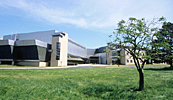
NIST’s new Advanced Measurement Laboratory is the most technically advanced research facility of its kind in the world. The $235 million, 49,843 square meter (536,507 square foot) facility features five separate wings with stringent environmental controls on air quality, temperature, vibration, and humidity. |
The AML includes sophisticated low-vibration "clean rooms." Here, materials researcher Stephen Hsu prepares to measure nanoscale friction between a diamond tip and a silicon surface. Such measurements are needed for the design of nanosized gears and other devices that will become the nanomachinery of the future. |
Physicist Thomas LeBrun uses a special joystick to manipulate nanowires with "optical tweezers." A highly focused laser beam attracts microscopic objects and can be used to pick up and precisely position nanocomponents for building semiconductor circuits or biosensors smaller than a red blood cell. Tools for manipulating nanocomponents will help accelerate research on the performance of new nanotechnologies.
|
Semiconductor nanocrystals are clusters of atoms about 10 nanometers or smaller that glow different colors depending on their size. Biophysicist Jeeseong Hwang holds a solution of red nanocrystals used to identify specific biomolecules. Hwang and his colleagues are measuring the optical properties of single nanocrystals to help medical researchers better calibrate tests using this new nanotechnology. Copyright is owned by the photographer. This photo is available without charge for use in materials that describe NIST programs directly. To receive a high resolution version of this image contact: inquires@nist.gov, (301) 975-6478.
|
Tight control of environmental factors in the AML makes it possible to improve calibrations for light-measuring devices. Here, physicist Jeanne Houston aligns a laser beam into the NIST primary optical standard used for calibrating photodetector devices that sense ultraviolet, visible, or infrared light. Photodetectors are used widely in scientific laboratories as well as in the lighting, aerospace, defense, and many other industries. Copyright is owned by the photographer. This photo is available without charge for use in materials that describe NIST programs directly. To receive a high resolution version of this image contact: inquires@nist.gov, (301) 975-6478. |
|
Coordinate measuring machines (CMMs) are used to precisely measure the dimensions of complex automotive and other product parts. Tight temperature control in the AML will allow NIST to improve the accuracy of its CMM calibration services and to conduct research into the complex effects of changing temperatures on CMM performance. Here, mechanical engineer Herb Bandy uses a CMM to measure the dimensions of a cylinder-shaped machined part. |
Ultraprecise electrical measurements require extremely stable temperature, humidity, and vibration control. In this photo, physicist Rand Elmquist fills a cryogenic chamber with liquid helium in preparation for measuring the international standard for electrical resistance--the quantum Hall effect. U.S. laboratories and manufacturers use NIST electrical standards and calibrations for all kinds of measurements from home electricity usage to electrocardiograms to gene-mapping. Copyright is owned by the photographer. This photo is available without charge for use in materials that describe NIST programs directly. To receive a high resolution version of this image contact: inquires@nist.gov, (301) 975-6478.
|
To continue to advance microchip technologies, scientists are studying ways to assemble individual molecules for use as active circuit components. In the AML laboratory shown above, postdoctoral researcher Lucile Teague inserts a sample into a scanning tunneling microscope to study the electrical behavior of organic molecules on a gold surface. |
|
Nobel laureate William Phillips leads a research group working in the AML that uses a "lattice" of laser beams to manipulate the quantum states of large collections of individual atoms, the potential 1s and 0s in a future quantum computer. Their experiments are sensitive to vibration, temperature, and humidity changes. Quantum computing may provide a revolutionary new way to decipher complex encoded messages and perform other calculations impossible with today's computers. Copyright is owned by the photographer. This photo is available without charge for use in materials that describe NIST programs directly. To receive a high resolution version of this image contact: inquires@nist.gov, (301) 975-6478.
|
Magnetic Monet. This graphic shows the magnetic "domains" within thin-film rings of a new advanced material for making non-volatile logic devices. Changes in color indicate changes in the direction of the magnetization of the material. Housed in an AML metrology wing 12 meters (40 feet) underground, the NIST-developed instrument that recorded this data is the highest resolution magnetic imaging instrument in the United States.
|
Explosive Hot Pad. An infrared image shows temperature variations as a round swipe cloth is heated to vaporize any explosive particles that may be present. Black/deep purple areas are about 40 degrees C, while yellow/white areas are about 200 degrees C. NIST chemists are developing standards and calibration services to help optimize equipment used at airports and other venues for detecting explosive materials. |
|
Quantum daisy. Twelve cobalt atoms arranged in a circle on a surface of copper produce a daisy-like pattern from the interference of electron waves. This image was made with a one-of-a-kind instrument that, acting autonomously, picks up and places individual atoms anywhere on a surface. NIST scientists are studying the quantum properties of different atom arrangements to help improve the design and fabrication of nanoscale devices. |
Magnesium oxide dice. NIST scientists are developing new three-dimensional chemical imaging methods. Using a scanning transmission electron microscope, a tilting stage, and sensitive detectors, NIST researchers can construct images that reveal both the chemical components and the complex shapes of crystal structures. This image shows cubes of magnesium oxide. Nanoscale particles of gold were deposited on the crystal faces to help define the surface topography.
|
Silicon Staircase. Steps of silicon serve as a natural ruler for measuring vertical dimensions. This silicon "target" has step heights ranging from tens to hundreds of nanometers leading down to a flat, single atomic layer measuring only 0.3 nanometer. The microscope used to make this image sits on an isolated concrete slab equipped with air springs to cancel out even minute vibrations that could ruin the nanoscale measurements. |
Magenta Microheater. A NIST-developed microheater device can be used to quickly detect toxic gases such as sarin or mustard gas. Slight variations in the thickness of the sensing film covering the microheater cause changes in color that have been enhanced in this micrograph. NIST researchers will use the AML's Nanofabrication Facility to make arrays of such microsensors tailored to sense specific chemicals at part per billion concentration levels. |
Rainbow Film. A rainbow of colors indicates the thickness of a clear, organic film used to mount microscopic particles. The deep blue and brown on the left of this optical micrograph show that the film is less than a micrometer thick, the right thickness for embedding single particles for microstructural analysis. In an AML ultraclean room, NIST chemists mount and analyze individual particles for forensic, advanced materials, and other researchers.
|
|
|
Created:
June 21, 2004 |
||