|
Nanotechnology
is an emerging, interdisciplinary area of research with
important commercial applications, and will, most assuredly, be a dominant
technology in new-world economies. As a general rule, nanotechnology addresses
our ability to understand and manipulate the physical and technological
characteristics that govern the behavior of a class of systems that possess at
least one physical dimension that is (typically) on the order of 100 nm or
less. More importantly, perhaps, is that when this is the case, it is often
observed that such systems may possess entirely new physical and chemical
characteristics that result in properties that are neither well described by
those of a single molecule of the substance, nor by those of the bulk material.
The new properties result from phenomena such as quantum confinement that
occurs in the nanoscale dimensions, and in many instances the origins of the
new properties are, at present, not fully understood. Our ability to exploit
these new properties for practical and useful gains lies in our ability to
understand the underlying physics that governs them. |
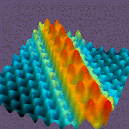
Image of single atomic zig-zag chain of Cs atoms (red) on the GaAs(110) surface. |
|
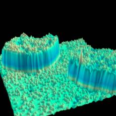
Image of substitutional Cr impurities (small bumps) in the Fe(001) surface. |
|
|
Nanotechnology has tremendous potential to change the present paradigms in U.S.
industry, including manufacturing, healthcare, materials, and electronics and
communications, and it offers tremendous opportunities for enhancements to U.S.
economic competitiveness. Accordingly, NIST is focusing on the development of
this technology's enabling infrastructure by developing critical measurement
techniques and standards that are essential to the wide deployment of
nanotechnology, including nanodevices, nanomagnetics, nanomanipulation and
nanocharacterization. As an example, in order to achieve high-volume production
rates in the manufacture of nanoscale devices, it is essential that the physics
governing self-assembly and self-replication be well understood. Accurate and
precise location of nanostructures and the measurement of the forces and
kinetics that govern self-assembly are needed to permit efficacious
implementation of any particular manufacturing strategy. NIST is developing
scanned-probe microscopy techniques that will permit detailed measurement of
the physical, electronic, and magnetic properties of various classes of
nanometer-scale structures, including quantum wires and dots. Further, we are
working on the method of autonomous atom assembly to fabricate atomically
perfect nanostructures for scientific study. |
| |
|
Within the NIST Physics Laboratory, the principal scientific efforts in
nanotechnology are being carried out within the Electron and Optical Physics
Division (now in CNST)
and the Quantum Physics Division.
The work of these two groups is focused on developing a detailed understanding
of the fundamental physical properties of nanometer-scale materials, and the
technical challenges that must be overcome in order to synthesize useful
quantities of nanomaterials and nanodevices for practical, industrial-scale
applications. |
|
|
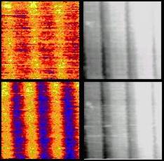
Infrared (left) and topographic (right) images of a photoresist
sample for two different infrared wavelengths (2.8 µm top, 2.95 µm
bottom). The different contrast observed for the two wavelengths demonstrates
chemical specificity. |


 Inquiries or comments:
Feedback
Inquiries or comments:
Feedback
Online: February 2001 - Last update: August 2007
|