Manufacturing Engineering Laboratory NIST logo
HOME About MEL Research products and services what's new search

Return to
Programs page

Projects

Measurement Methods and Calibrations

International Comparisons and Standards

Optical Metrology for the Semiconductor Industry

Measurement and Calibration of Nano-Structured Optical Elements


PDF of Program write-up


melwebmaster

Date created:
March 28, 2008
Last updated:
May. 07, 2008

Return to top

Return to top

Return to top

Return to top

Return to top

Return to top

NIST IR3 infrared interferometer measuring the thickness variation of a 300 mm diameter silicon wafer
collimator wafer

Manufacturing Metrology Division Program

Advanced Optics Metrology Program

Annual FTEs: 2.0 NIST staff

3.0 guest researchers

5.0 total FTEs

Challenge:

Provide methods, measurement services, and standards for SI-traceable metrology of optical figure and wavefront that contribute to innovations in the application and manufacture of optical elements and precision surfaces.

Overview

Optical technology is an enabling technology in many areas. Communication, bio-medical imaging, defense, astronomy, nano-scale manufacturing, semiconductor manufacturing, and many other applications depend crucially on optical systems. Manufacturing these optical systems depends in turn on the ability to measure their performance, which requires traceable metrology for optical figure and wavefront. In high-impact applications such as semiconductor lithography, uncertainties are at the demanding sub-nanometer level. Few standards exist in this area. Traceability requires standards-compliant uncertainty statements (i.e., based on the GUM – Guide to Uncertainty in Measurement) that are rare in the U.S. optics industry, but increasingly mandated for ISO-certified quality systems and export. Only a small number of very specialized optical companies practice the metrology of aspheric and nano-structured optical elements. No general, widely-recognized, validated way exists to calibrate these optical elements, and the application range and uncertainty of existing methods are poorly understood. This has hindered the manufacture and adoption of these optical elements, despite their ability for game-changing product innovations.

The program addresses infrastructural metrology challenges faced by U.S. industry and other federal agencies through:

  1. Measurement methods and calibration services for optical figure of flat, spherical, and aspherical precision surfaces that provide innovation leverage, have deep metrological penetration into the U.S. metrology chain, or are mission critical. Where possible, we develop protocols that allow users to make (absolute) calibrations in their own facilities.
  2. International comparisons and harmonized standards for optical figure and wavefront metrology that ensure effective access to international markets by the U.S. optics industry.
  3. Measurement methods and reference artifacts for silicon wafer flatness and extreme ultraviolet lithography (EUVL) optical elements that address future requirements of the International Technology Roadmap for the Semiconductor Industry (ITRS).
  4. Measurements and calibrations that support the manufacture and adoption of nanostructured optical components by U.S. industry.

Key Accomplishments and Impacts:

  • Developed and characterized methods for absolute calibration of optical flats, taking into account variability of mounting induced deformations, in response to requests from leading U.S. optics manufacturers and research institutions for full-surface flat calibrations with low uncertainties. Realized ability to calibrate 300 mm flats with a standard uncertainty of 0.2 nm rms, and executed NIST special tests for customers.
  • Initiated an international comparison of flatness metrology and developed the corresponding protocol and test artifact.
  • Characterized and improved uncertainty of radius of curvature measurements (20 nm for 100 mm radius) and absolute measurement of sphericity in response to customer requests, and provided special tests for customers.
  • Developed and characterized an experimental system for estimating form errors of freeform and aspheric surfaces from measurements of local curvature.
  • Developed and characterized an infrared interferometer (1552 nm) for measuring the thickness variation of 300 mm silicon wafers with a standard uncertainty of 5 nm in response to the needs of manufacturers of silicon wafers and related metrology tools. We produced reference wafers with a calibrated thickness variation that enable users and manufacturers of wafer inspection tools to evaluate and improve measurement performance. Using our measurements, a U.S. company developed a process to manufacture ultra-flat wafers that meet ITRS site flatness requirements well into the next decade.
  • In collaboration with NASA, developed metrology methods and designed diffractive optical elements to calibrate the form of mandrels used to shape aspheric mirrors for future X-ray telescopes, and conducted process characterization experiments for their fabrication in the NIST NanoFabrication facility.

Future Directions and Plans:

Our measurement capability for flatness, sphericity, radius of curvature, and wafer thickness variation is mature. Future work will focus on the uncertainty analysis and comparison of measurement techniques for aspheres and nano-structured optical elements, and will address needs of collaborators such as NASA that are currently not met by industry.

Awards and Recognition

  • Ulf Griesmann joined the Optics and Electro-Optics Standards Council, a forum of technical experts that provides guidance on behalf of the U.S. for national and international standards in the areas of optics and optical measurements. [November 2007]
  • Ulf Griesmann served as the General Chair of the Optical Society of America (OSA) Topical Meeting on Optical Fabrication and Testing, 2006, Rochester, NY. He will Co-Chair this meeting in 2008.

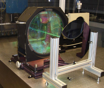
Projects

Advanced Optics Metrology Program

Measurement Methods and Calibrations
(Status: to be completed in FY2010)

Challenge/Problem Addressed:

Flat and spherical reference surfaces are key components in the traceability chain of interferometric measurements of optical figure and wavefront. The ability to perform absolute calibrations of these surfaces with uncertainties at the nanometer-level or below powerfully enhances the ability of the optics industry to manufacture and measure high-performance optical systems.

To achieve high optical performance, low system weight, and low cost, modern optical systems increasingly use aspheric surfaces. However, measuring aspheric surfaces poses formidable metrology problems because of the difficulty of obtaining a reference wavefront that closely matches the desired form of the asphere. No single, widely recognized, general, validated way exists for calibrating or measuring complex surfaces with nm-level uncertainties. Common techniques are general interferometry using “stitching” methodology or refractive or diffractive “null” optics (e.g., computer generated holograms (CGH)). The application range and uncertainties of these techniques are poorly understood.

Objective

Provide full-aperture measurement methods and calibration services for optical figure of flat, spherical, and aspherical precision surfaces with state-of-the-art accuracies, focusing on calibration services for flatness, sphericity, and radius of curvature of optical surfaces with an aperture up to 300 mm, and specifications for the application range and achievable uncertainties of various measurement methods, including stitching, computer generated holograms, shearing interferometry, and measurements of local curvature.

Accomplishments:

  • Developed, characterized, and published methods for the absolute calibration of optical flats based on the three-flat concept, including the effect of gravity-induced flat deformations on calibration uncertainty. Measurements were augmented with finite element analyses of the variation in flatness errors that occur in a rotated flat due to rotational asymmetries in the flat mount and flat geometry.
  • Characterized the uncertainty of absolute sphericity measurements using the ball averaging method and published the results.
  • Completed phase I of the experimental geometric measuring machine (GEMM) system to estimate form errors of freeform and aspheric surfaces from measurements of local curvature. Published an uncertainty evaluation for profile measurements which included a comparison showing excellent consistency in measurements of the form of an elliptical synchrotron mirror obtained with the NIST Moore M48 CMM, stitching interferometry, and slope-based optical profiling. Developed a new algorithm for the estimation of 3D surfaces from curvature measurements. Realized a novel curvature measurement sensor with integrated standoff measurement capability to reduce measurement uncertainties; the sensor is being integrated into the GEMM system.
  • Provided full-aperture calibrations (NIST special tests) for flatness, sphericity, and radius of curvature to customers.

Planned Future Accomplishments:

  • Realize capability for the calibration of radius and form errors of spherical reference surfaces with radii larger than 100 mm as requested by leading optics companies. Characterize the uncertainty of common calibration methods for reference spheres.
  • Address the challenge of characterizing, with low uncertainties, the radius and form errors of spherical surfaces with large radii (10 m to 1000 m) through the application of diffractive optics.
  • Complete study to resolve conflicting opinions in industry on the uncertainties of the stitching approach used to extend measurement area or enable asphere measurement (including effects of retrace errors and errors in reference wavefront and image registration).

Customers and Collaborators:

  • QED Technologies
  • Argonne National Laboratory / Advanced Photon Source
  • NASA
  • Zygo
  • Zeiss IMT
  • ITT Space Systems Division

Advanced Optics Metrology Program

International Comparisons and Standards
(Status: to be completed in FY2009)

Challenge/Problem Addressed:

Controversies on measurement procedures, specification compliance, and traceability continue to hamper international commerce in advanced optical elements. Standards-compliant uncertainty assessments (i.e., based on the GUM – Guide to Uncertainty in Measurement) are rare in the optics industry. Companies increasingly need to adopt ISO-certified quality procedures, especially for goods that are exported. Having traceable in-house metrology with well-documented uncertainty statements is thus becoming essential to optics and precision engineering companies.

Objective

Ensure effective access to international markets by the U.S. optics industry through international comparisons and harmonized standards for optical figure and wavefront.

Accomplishments:

  • Initiated an international comparison of flatness measurements of 300 mm diameter optical flats, with NIST acting as the pilot laboratory. Procured and characterized the comparison artifact. Designed and realized an instrumented shipping container and a test mount sleeve that allows the artifact to be measured in both vertical and horizontal orientations.

Planned Future Accomplishments:

  • Complete international comparison of flatness measurements (FY2009)
  • Contribute to the ANSI Optics and Electro-Optics Standards Council (OEOSC) Technical Advisory Group to ensure that international standards reflect the state-of-the-art.

Customers and Collaborators:

Comparison Participants

  • CSIRO (Australia)
  • NPL (UK)
  • NMIJ (Japan)
  • KRISS (Rep. of Korea)
  • and PTB (Germany)

Advanced Optics Metrology Program

Optical Metrology for the Semiconductor Industry
(Status: to be completed in FY2010)

Challenge/Problem Addressed:

As exposure tools for optical lithography evolve toward larger numerical apertures, the semiconductor industry expects continued demand for improved wafer flatness at the exposure site. The allowable site flatness error for 300 mm wafers is expected to be less than 50 nm by 2010 and may be as low as 25 nm by 2015, according to the International Technology Roadmap for Semiconductors (ITRS 2006). These goals present a challenge for both wafer polishing and metrology tools.

Advances in lithography are crucial to continued growth in the semiconductor industry. The introduction of extreme ultraviolet lithography (EUVL) as the manufacturing process for next-generation semiconductors has been delayed by the low lifetime of EUVL reflective optics (more than a factor of 100 below what is required). Since optimal resolution requires the figure of the optics to be within a fraction of the operational wavelength, EUVL optical components must be fabricated to sub-nanometer tolerances and retain stability over several years of exposure. The effects of EUV exposure on long-term dimensional stability and phase change characteristics of EUV-reflective surfaces are largely unknown.

Objective

Provide measurement methods and reference artifacts for silicon wafer thickness variation and EUVL optical elements that address requirements of the International Technology Roadmap for the Semiconductor Industry (ITRS).

Accomplishments:

  • Completed development and characterization of the NIST infrared interferometer (1552 nm) for measuring the thickness variation of 300 mm silicon wafers with an uncertainty of 5 nm.
  • Produced reference wafers with calibrated thickness variation that enable users and manufacturers of wafer inspection tools to evaluate and improve measurement performance.
  • Provided measurements that enabled a U.S. company to develop a corrective sub-aperture polishing process to manufacture ultra-flat wafers that meet ITRS site flatness requirements well into the next decade.

Planned Future Accomplishments:

  • Evaluate the uncertainty that can be achieved with a shearing interferometer operating at EUV wavelengths by building a prototype interferometer working with visible light and comparing its performance against phase shifting interferometry.
  • Produce measurement data to clarify the effects of EUV exposure on the lifetime of EUV reflective optics (anticipated future activity).

Customers and Collaborators:

  • QED Technologies
  • MEMC Electronic Materials Inc.
  • Wavefront Sciences

Advanced Optics Metrology Program

Measurement and Calibration of Nano-Structured Optical Elements
(Status: to be completed in FY2010)

Challenge/Problem Addressed:

Modern micro-fabrication technology has made possible the precise fabrication of three-dimensional structures that are small compared to the wavelength of light. This capacity opens up new ways to engineer the phase and amplitude of light waves to create light waves with unique properties, leading to the emergence of a new class of optics commonly referred to as “diffractive optics” to emphasize that device function is achieved through the scattering of light by microscopic structures with dimensions comparable to the wavelength of light. Diffractive optical elements (DOEs) have properties that traditionally polished optics cannot achieve. For example, a diffractive lens can focus a light wave at several points in space simultaneously. DOEs are therefore important components in many novel optics products and they have become a vibrant field of research. They can also improve the calibration of optical elements with aspheric surfaces. The NIST NanoFabrication facility provides unique resources for the fabrication of DOEs.

Objectives

Provide methods and capability for traceable measurement of wavefronts using customized diffractive optical elements. Provide documented methods to calibrate wavefronts generated by nano-structured optical elements that support the manufacture and adoption of nanostructured elements by U.S. industry.

Accomplishments:

  • In collaboration with NASA, developed metrology methods and designed diffractive optical elements to calibrate the form of mandrels used to shape aspheric mirrors for future X-ray telescopes. Conducted
    preliminary process characterization experiments for fabrication of the
    diffractive optical elements in the NIST NanoFabrication facility.
  • In collaboration with NASA, fabricated and characterized a phase resolution target to evaluate the spatial frequency response of surface interferometers.

Planned Future Accomplishments:

  • Develop a prototype optical test based on computer-generated holograms to calibrate the form errors of mandrels used to shape aspheric mirrors for future X-ray telescopes.
  • Develop methods to calibrate wavefronts generated by nano-structured optical elements and characterize the relation between wavefront and fabrication errors.

Customers and Collaborators:

  • NASA Goddard Space Flight Center
Manufacturing Engineering Laboratory Skip navigation