|
August
30, 2004

[NIST
Tech Beat Search] [Credits] [NIST Tech Beat
Archives] [Media
Contacts] [Subscription Information]

Chip-Scale
Atomic Clock Unveiled by NIST
 |
 |
NIST
physicist John Kitching displays the heart of the world’s
smallest atomic clock. This “physics package” is
about the size of a grain of rice.
© Geoffrey Wheeler
To
receive a high-resolution version of this image, contact Gail
Porter. |
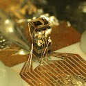
The
“physics package” of the chip-scale atomic clock
includes (from the bottom) a laser, a lens, an optical attenuator
to reduce the laser power, a waveplate that changes the
polarization of the light, a cell containing a vapor of
cesium atoms, and (on top) a photodiode to detect the laser
light transmitted through the cell. The tiny gold wires
provide electrical connections to the electronics for the
clock.
NIST Photo |
The
heart of a minuscule atomic clock—believed to be
100 times smaller than
any other atomic clock—has been demonstrated by
scientists at the National Institute of Standards and
Technology (NIST),
opening the door to atomically precise timekeeping in portable,
battery-powered devices for secure wireless communications,
more precise navigation and other applications.
Described
in the Aug. 30, 2004, issue of Applied Physics Letters,*
the clock’s inner workings
are about the size of a grain of rice (1.5 millimeters on a
side and 4 millimeters high), consume less than 75 thousandths
of a watt (enabling the clock to be operated on batteries)
and are stable to one part in 10 billion, equivalent to
gaining
or losing just one second every 300 years.
In addition,
this “physics package” could be fabricated and assembled
on semiconductor wafers using existing techniques for making
micro-electro-mechanical systems (MEMS), offering the potential
for low-cost mass production of an atomic clock about the size
of a computer chip and permitting easy integration with other
electronics. Eventually, the physics package will be integrated
with an external oscillator and control circuitry into a finished
clock about 1 cubic centimeter in size.
The mini-clock is
comparable in size and long-term stability to temperature-compensated
quartz crystal oscillators, currently used in portable devices.
NIST scientists expect to improve the clock’s long-term
stability and reduce its power consumption to the point where
the device could substantially improve the performance of many
commercial and military systems that require precision time
keeping.
For more
information see: www.nist.gov/public_affairs/releases/miniclock.htm.
Media
Contact:
Laura
Ost, laura.ost@nist.gov,
(301) 975-4034
*S. Knappe,
V. Shah, P. Schwindt, L. Hollberg, and J. Kitching. 2004.
A microfabricated atomic clock. Applied Physics Letters 859(9),
Aug. 30.

Software
Difficulties Cost Builders Billions
Inadequate
software interoperability in the capital facilities
industry
cost the commercial, institutional and industrial building
sectors $15.8 billion in 2002 in lost efficiency,
according
to a newly released study commissioned by the National Institute
of Standards and Technology (NIST).
Conducted
by RTI International (Research Triangle Park, N.C.) and
the Logistics
Management Institute (McLean, Va.), the report places a price
tag on avoidance, mitigation and delay activities due
to data-exchange
problems. It also takes into account the cost of redundant
paper management.
The analysis, expected
to benefit key stakeholders throughout the construction industry,
breaks down data exchange-related losses for architects and
engineers, general contractors, specialty fabricators and
suppliers, and owners and operators at three different stages
of a building’s life: (1) design and engineering; (2)
construction; and (3) operations and maintenance.
The
publication, Cost Analysis of Inadequate Interoperability
in the
U.S. Capital Facilities Industry (NIST GCR 04-867),
also identifies barriers and opportunities for improvement.
Electronic copies are available at www.bfrl.nist.gov/oae/oae.html.
Media
Contact:
John
Blair, john.blair@nist.gov,
(301) 975-4261
Patented
Process Preserves Transplant Tissues/Organs
Body
tissues such as blood vessels, cartilage and skin—even
whole organs such as kidneys, livers and hearts—could
become more widely available for transplants as a result of
a patent issued recently to Organ Recovery Systems of Chicago
for a method to chill body tissues and organs well below freezing
without forming ice crystals. The new process for tissue "vitrification"—chilling
tissue and organs to a disordered, glass-like solid without
ice formation—was developed with support from the National
Institute of Standards and Technology (NIST) Advanced Technology
Program and the National Institutes of Health.
There
is an urgent need for tissues and organs for transplantation.
Doctors conducted
over 24,000 organ transplants in the United States in 2002;
yet someone is added to the donor waiting list every 12
minutes
and 16 people die each day waiting for an organ transplant.
A significant roadblock to the broader use of transplantation,
regardless of the source (donated human, cross-species or
artificial), has been the problem of preserving the transplant
tissue. Better preservation techniques would allow transplant
materials to be shipped anywhere in the world or, better
yet,
collected and stored in something akin to blood banks until
needed.
Organs
and some tissues are presently stored for short periods
at refrigerator
temperatures (approximately 4 °C) and freezing has not
been possible due to ice crystals, which damage delicate
cells
and greatly reduce the viability or functions of the tissue.
Chemicals called cryoprotectants reduce ice formation but
have toxic effects that introduce their own problems. The
Organ Recovery Systems technique combines a mixture of cryoprotectant
compounds that cancel each other’s toxicity and careful
control of the cooling and warming processes to minimize
damage
to the tissue. The technique is discussed in U.S. patent
no. 6,740,484. (Patent
text available at www.uspto.gov.)
Media
Contact:
Michael
Baum, michael.baum@nist.gov,
(301) 975-2763
Scientists
Observe 'Atomic Air Force'
The
first sighting of atoms flying in formation has been reported
by physicists at the Department of Commerce’s National
Institute of Standards and Technology (NIST) and the University
of Colorado at Boulder (CU-Boulder) in the Aug. 13 issue of
Physical Review Letters.* While the Air Force and geese prefer
a classic “V,” the strontium atoms—choreographed
in this experiment with precision laser pulses and ultracold
temperatures—were recorded flying in the shape of a cube.
This “really bizarre” behavior is believed to occur
with all atoms under similar conditions, says physicist Jun
Ye of NIST, who led the research at JILA, a joint institute
of NIST and CU-Boulder. Ye is also a faculty member of the CU-Boulder
physics department.
Atoms have not previously been seen flying in formation, says
Ye. Strontium’s unique physical properties make the observations
possible. In particular, the configuration of strontium’s
electrons and the resulting atomic properties allow it to efficiently
absorb laser energy in two very specific “resonant”
wavelengths—a strong resonance at a wavelength of blue
light and another, much weaker resonance for longer-wavelength
red light. This makes strontium a promising candidate for a
next-generation atomic clock based on optical rather than microwave
frequencies, and is the reason the JILA team is studying the
atom’s quantum behavior.
The
experiment was conducted with a dense gaseous cloud of 100 million
strontium atoms. The atoms were trapped in the center of a vacuum
chamber with both a magnetic field and six intersecting red
laser beams, in three sets of facing pairs aligned at right
angles to each other. The NIST group coaxed the atoms into the
flying cube formation with precise adjustments in the frequency
of the laser beams used to trap them. The formation was visualized
by illuminating the atoms with a blue laser. The strontium absorbed
the energy but then quickly re-emitted it and the clusters of
glowing blue atoms were recorded with a video camera.
For
further information, see www.nist.gov/public_affairs/releases/atomic_airforce.htm.
Media
Contact:
Laura
Ost, laura.ost@nist.gov,
(301) 975-4034
*T.H.
Loftus, T. Ido, A.D. Ludlow, M.M. Boyd, and
J. Ye. 2004. Narrow line cooling: finite photon recoil
dynamics. Physical Review Letters 93(7), Aug. 13.
Supercool!
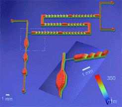
Model Unscrambles Complex Crystallization Puzzle
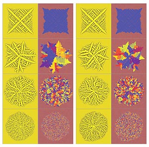 |
Four
sets of simulation images show the striking similarities
between crystals "grown" under different conditions.
The first two columns on the left show
crystals grown with increasing amounts of impurities.
The top row crystal has no "dirt," it has
a symmetric crystal pattern (yellow image) and it has
no "grains"— all the molecules are aligned
in the same direction (blue image.) As greater amounts
of impurities are added, the crystal grows more and
more randomly.
The two
columns on the right show crystals grown with
increasing differences
between the speed the crystal
naturally wants to grow and the speed that liquid
molecules can rotate into alignment with the growing
crystal
or be forced to solidify into a new grain. This
type of difference happens in the real world when
liquid
alloys or polymers are supercooled substantially
below the temperature that they would naturally solidify.
The low temperature tends to speed up the crystallization
process but the increasing viscosity of the liquid
makes it harder for molecules to move into aligned
grains, so the crystal grows more randomly. |
To
the wonderment—and the befuddlement—of scientists,
the patterns that form as plastics, metals and many other
materials crystallize can vary incredibly, ranging from sea-urchin-like
spheres to elaborate tree-like branches.
Now,
Hungarian and National Institute of Standards and Technology
scientists report in the September issue of Nature Materials*
that they have developed a way to predict the polycrystalline
microstructures that will form as complex liquid mixtures
cool and solidify. Ultimately, the team's new simulation
tool
could help manufacturers of everything from plastic bags
to airplane wings to design new products with improved strength,
durability and other properties.
Images
generated with the team's mathematical model match up
almost feature
for feature with the seemingly random crystal patterns formed
in experiments as temperatures or other processing variables
are modified. The model accurately predicts how both impurities
(or additives) and process differences affect the sizes,
shapes
and orientations of crystals that form during the so-called
supercooling process.
Whether
initiated by "dirt" or by processing conditions,
the resulting patterns can be strikingly similar. This "duality
in the growth process," notes NIST’s James
Warren, may help explain why polycrystalline growth patterns
are so
prevalent in polymers and other materials derived from complex
mixtures.
Findings
based on the model indicate that instabilities along the boundary
between liquid and solid areas during solidification effectively
clash with the otherwise orderly process of crystallization.
Tiny crystals-in-the-making move and position themselves along
the growth front, assuming an orientation peculiar to the
energy conditions at their location. Varying local conditions
produce crystals in seemingly disordered arrays, accounting
for the rich diversity of microstructural patterns.
Laszlo Granasy, of
Hungary’s Research Institute for Solid State Physics and
Optics, led the research effort.
*L.
Gránásy, T. Pusztai, T. Börzsönyi, J.A.
Warren, and J.F. Douglas. A general
mechanism of polycrystalline growth. 2004. Nature
Materials advance on-line publication, Aug. 8, 2004.
Media
Contact:
Mark Bello, mark.bello@nist.gov,
(301) 975-3776
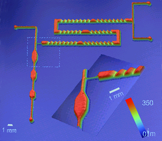
New
Microfluidic Device Tackles Tough Synthesis Tasks
A
new type of microfluidic device
that can help industry to optimize paints, coatings
for microelectronics and specialty polymers has
been
developed by National
Institute of Standards and Technology (NIST) researchers.
The device is made of a chemically durable plastic
that is resistant to many common organic solvents.
It was fabricated with a rapid prototyping method
also developed at the agency.
 |
NIST
microfluidic device for synthesizing and
analyzing polymers and other complex liquids.
|
Described
in the Aug. 18 issue of the Journal of the
American Chemical Society,* such devices can be used to make
specialty polymers in small amounts, or to rapidly
change polymer ingredients so that the impact of
expensive additives on material behavior can be
systematically analyzed. This is becoming important
as more specialty polymers use designer elements
for applications in nanotechnology and biotechnology.
Devices
typically measure about half the size of a credit
card and are made with a technique called "frontal
photopolymerization." The NIST researchers
adapted the technique to fabricating microfluidic
devices. Ultraviolet light was shined through patterned
"stencils" into a liquid layer of a chemical
called thiolene. Areas exposed to the light harden
into a solid polymer while unexposed areas remain
liquid and can be flushed away, leaving relatively
deep channels capable of handling thicker fluids
than current lab-on-a-chip devices.
In
a separate paper,** the NIST researchers provide
detailed data about how varying doses of ultraviolet
light affect the height of the polymer structures
formed. Such data should be helpful for increasing
the complexity of devices that can be fabricated
with the technique.
Media
Contact:
Scott Nance,
scott.nance@nist.gov,
(301) 975-5226
*T. Wu, Y. Mei, J.T. Cabral,
C. Xu, and K.L. Beers. 2004. A new synthetic
method for controlled polymerization using a microfluidic
system. Journal of the American Chemical Society.
[http://polymers.msel.nist.gov/publications/]
**J.T. Cabral, S.D. Hudson, C.
Harrison, and J. Douglas. 2004. Frontal photopolymerization
for microfluidic applications. Langmuir.
Expected print publication in Nov. [http://polymers.msel.nist.gov/publications/]
Lighting
the Way to Better Nanoscale Films
Most
miniature electronic, optical and micromechanical
devices are made from expensive semiconductor or
ceramic materials. For some applications like
diagnostic
lab-on-a-chip devices, thin-film polymers may provide
a cheaper alternative, but the structure and
properties
of these materials—often no more than a few
nanometers (nm) thick—are difficult to determine.
In addition, defects in the thin polymer masking
materials used to "print" integrated
circuits can produce malfunctioning components.
Consequently,
researchers would like to have a
non-invasive
method for scanning polymer films for defects at
high resolution.
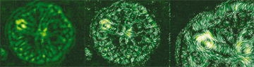 |
Left: The
crystal structure of a thin-film polymer "seaweed" crystal
that is about four micrometers wide.
Brighter
areas indicate parts of the crystal with
the greatest "strain." Center: The
same crystal with lines superimposed showing
the direction of strain between
the crystal's atoms. Right: Closeup
of the upper left portion of the center
image.
|
In
the Aug. 23 issue of Applied Physics Letters,*
researchers at the National Institute of Standards
and Technology (NIST) report on an application
of a new method for studying ultrathin polymers
that
makes it possible to visualize defects and structure
in these materials and should help improve
basic
understanding of crystal formation in polymers.
Using
a special form of near-field scanning optical
microscopy, the NIST researchers were able to
determine the structure of, and "strain" (stretching
between atoms) in, thin-film crystals of polystyrene.
Polystyrene is a ubiquitous plastic found in foam
cups, CD cases and many other products.
The
films examined formed tiny crystals just 15
nm thick
and about 1500 nanometers wide, which makes
them difficult to study with other optical microscopes.
In the NIST experiments, blue-green light was piped
through a glass fiber about 50 nm wide and scanned
across the sample about 10 nm above the surface.
Changes in the polarization of the light (the
direction
of the wave's electric field) as it transmits through
the sample then were used to investigate the
material's
crystal structure and to map areas of strain.
The
NIST results should help scientists choose and improve
polymer materials and processes for fabricating
a range of microscale and nanoscale plastic devices.
Media
Contact:
Gail Porter,
gail.porter@nist.gov,
(301) 975-3392
*L.S.
Goldner, S.N. Goldie, M.J. Fasolka, F. Renaldo,
J.
Hwang, and J.F. Douglas. 2004. Near-field polarimetric
characterization of polymer
crystallites. Applied Physics Letters 85(8):
1338-1340.
Fire Tests Provide WTC Floor System Data
During
the month of August, the National Institute of Standards
and Technology
(NIST) conducted a series of four fire resistance tests
on composite concrete-steel trussed floor systems typical
of those used in the World Trade Center (WTC) towers.
The tests showed that the test structures were able to
withstand standard
fire conditions for between one and two hours. Part of
NIST’s building and fire safety investigation of
the WTC disaster on Sept. 11, 2001, the four tests provide
only a means for evaluating the relative fire resistance
rating of the floor systems under standard fire conditions
and according to accepted test procedures. The tests
alone cannot be used to determine the actual performance
of the
floor systems in the collapse of the WTC towers. To learn
more about what the tests revealed, go to www.nist.gov/public_affairs/factsheet/wtc_fire_resistance_data.htm.
Checklists
for Computer Security
The
National Institute of Standards and Technology (NIST),
with sponsorship
from the Department of Homeland Security (DHS), has issued
a new report, Draft NIST Special Publication 800-70: Security
Configuration Checklists Program for IT Products.
The use of computer security checklists, when combined
with well-developed
guidance, leveraged with high-quality security expertise,
vendor product knowledge, operational experience,
and accompanied
with tools, can reduce markedly the vulnerability exposure
of an organization. The report gives an overview of
the
NIST Checklist Program, explains how to retrieve checklists
from NIST's repository and provides general information
about threat models and baseline technical security policies
for associated operational environments. The report
is available
at http://csrc.nist.gov/checklists/index.html.
Building
Brains for Thinking Machines
James
S. Albus, a Senior Fellow at the National Institute of Standards
and Technology (NIST) described efforts to develop "thinking
machines" last month in Portugal at the International
Federation of Automatic Control Symposium on Intelligent
Autonomous Vehicles. Albus, who predicts that autonomous
vehicles could equal human levels of performance in most
areas within 20 years, is the co-inventor of the Real-time
Control Systems (RCS) architecture and methodology. Albus
described how computer modeling, value judgment, sensory
processing and knowledge databases and programs may be used
to mimic human thought processes. Albus’ address on
the artificial intelligence framework and its current and
future field applications is at http://www.isd.mel.nist.gov/documents/albus/RCS_Cognitive_Arch.pdf.
(Return
to NIST News Page)
Editor:
Gail Porter
Date
created:08/26/04
Date updated:08//04
Contact: inquiries@nist.gov
|