Joseph
Stroscio; Robert Celotta / NIST |
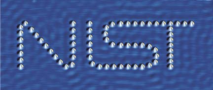
A
40-nanometer-wide NIST logo made with cobalt atoms on
a copper surface. The ripples in the background are made
by electrons, which create a fluid-like layer at the copper
surface. Each atom on the surface acts like a pebble dropped
in a pond.
Click
on image for high-resolution
version. |
In an
effort to put more science into the largely trial and error
building of nanostructures, physicists at the Commerce Department's
National Institute of Standards
and Technology (NIST) have demonstrated new methods for
placing what are typically unruly individual atoms at precise
locations on a crystal surface.
Reported
in the Sept. 9, 2004, online version of the journal Science,
the advance enables scientists to observe and control, for
the first time, the movement of a single atom back and forth
between neighboring locations on a crystal and should make
it easier to efficiently build nanoscale devices "from
the bottom up," atom by atom.
The NIST
team was surprised to find that the atoms emitted a characteristic
electronic "noise" as they moved between two different
types of bonding sites on the crystal surface. By converting
this electronic signal into an audio signal, the researchers
were able to "hear" the switching take place. The
sound resembles a hip hop musician’s rhythmic "scratching"
and can be used by researchers to know in real time that atoms
have moved into desired positions.
Several
research groups already are using specialized microscopes
to build simple structures by moving atoms one at a time.
The NIST advance makes it easier to reliably position atoms
in very specific locations. "What we did to the atom
is something like lubricating a ball bearing so that less
force is required to move it," says Joseph Stroscio,
co-author of the Science paper.
Such
basic nanoscale construction tools will be essential for computer-controlled
assembly of more complex atomic-scale structures and devices.
These devices will operate using quantum physics principles
that only occur at the atomic scale, or may be the ultimate
miniaturization of a conventional device, such as an “atomic
switch” where the motion of a single atom can turn electrical
signals on and off.
The research
involved using a custom-built, cryogenic scanning tunneling
microscope (STM) to move a cobalt atom around on a bed of
copper atoms that are closely packed in a lattice pattern.
In a typical STM, a needle-like tip is scanned over an electrically
conducting surface and changes in current between the tip
and the surface are used to make three-dimensional images
of the surface topography. The tip can be brought closer to
the surface to push or pull the cobalt atom.
In the
research described in Science, NIST scientists discovered
that the cobalt atom responds to both the STM tip and the
copper surface, and that the atom “hops” back
and forth between nearby bonding sites instead of gliding
smoothly. With slight increases in the current flowing through
the tip to the atom, the researchers were able to make the
cobalt atom heat up and vibrate and weaken the cobalt-copper
bonds. This induced the cobalt atom to hop between the two
types of lattice sites, with the rate of transfer controlled
by the amount of current flowing.
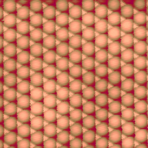
Joseph
Stroscio; Robert Celotta / NIST |
Colorized
version of an image created by the NIST custom-built
scanning tunneling microscope as it drags a cobalt
atom
across a closely packed lattice of copper atoms. Large
round features show the cobalt atom bonding to
the copper
at its preferred, lowest energy bonding site. Bright
triangle-shaped areas show the atoms bonding at
a higher
energy site. The atom "screeches in protest"
when the STM tip forces it to sit at this site. Dark
areas show positions that the atom "hops" over,
refusing to bond at all.
Click
on image for high-resolution
version.
|
The NIST
researchers also found that they could use the STM tip to
reshape the energy environment around the cobalt atom. This
allows control over the amount of time the cobalt atom spends
in one of the lattice sites. Using this technique the researchers
found they can even trap the cobalt atom in a lattice site
that the atom normally avoids. Sounds of the “protesting”
atom give rise to the “hip hop” scratching sound
described in Science.
“The
impact of the work is twofold,” says Stroscio. “We
learned about the basic physics involved in atom manipulation,
which will help us build future atomic-scale nanostructures
and devices. We also learned that we can control the switching
of a single atom, which has potential for controlling electrical
activity in those devices.”
The experiments
represent initial steps in exploring a new system of measurement,
atom-based metrology, in which single atoms are used as nanoscale
probes to collect information about their environment. In
particular, the NIST-built instrument can be used to draw
detailed maps of binding sites on a metal surface that cannot
be made with standard STM measurements.
The new
results are among the earliest to be published based on work
performed at NIST’s nanoscale physics facility, where
scientists are using a computer-controlled STM to autonomously
manipulate and control individual atoms, with the intent to
build useful devices and nanostructures. More information
on the facility is available at the following address: http://cnst.nist.gov/Facilities/nano_phy.html.
The work
was supported in part by the Office of Naval Research.
As a
non-regulatory agency of the U.S. Department of Commerce’s
Technology Administration, NIST develops and promotes measurement,
standards and technology to enhance productivity, facilitate
trade and improve the quality of life.
**J.A. Stroscio and R.J. Celotta. 2004. Controlling the Dynamics of a Single Atom in Lateral Atom Manipulation. Science Express, Sept. 9.
|