
|
||
|
Technology at a Glance is a quarterly newsletter from the National Institute of Standards and Technology reporting on research results, funding programs, and manufacturing extension and technology services. If you have comments or general questions about this newsletter or if you would like to receive the four-page, color newsletter in hard copy, please email your mailing address to Gail Porter, editor, or call (301) 975-3392. About Technology at a Glance. [Technology at a Glance Search] [Technology at a Glance Archives] |
||
|
|
||
|
||
|
|
||
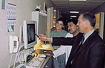
Video Standard Aids RadiologistsIn conjunction with the Video Electronics Standards Association, NIST has spearheaded an international flat-panel display measurement standard, which, in turn, has become the basis for how flat-panel measurements are made worldwide. Manufacturers, suppliers, and consumers of the technology are benefiting. The standard
specifies how performance measures such as contrast ratios or color
measurements for flat-panel displays should be conducted. Having a
single set of agreed-on standard measures makes it possible to objectively
compare the performance of flat-panel systems made by different manufacturers. In one case,
the standard was used by the Mayo Clinic Scottsdale (Ariz.) to specify
the purchase of 1,000 flat-panel displays for radiology. This allowed
the clinic to replace printed X-rays with digital images viewed on
flat-panel displays, a move that saves the clinic at least “The use of X-ray film has remained unchanged for 40 to 50 years,” says Dr. William Pavlicek of the Mayo Clinic. There is “enormous confidence” in the old technology. The new standard made it possible, he says, for the clinic to purchase flat-panel displays knowing that they could adequately duplicate the picture quality of film. With the new system in place, a radiologist at any one of the Mayo Clinic’s six locations throughout the Phoenix area (see photo above) can interpret an X-ray and send a response to a patient’s primary doctor within 60 seconds. A speech recognition system allows the radiologist to attach an official report to the digital X-ray without having to type in the data. About once a year the flat panels are re-calibrated according to the video standard to ensure that they produce consistent picture quality. The new standard
also has helped the aerospace and automotive industries. Aircraft
Contact: Ed Kelley, (301) 975-3842.
|
||
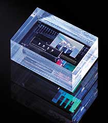
Integrating Optics With Electronics
Optical fibers, with their huge data-transfer capacities, are becoming pervasive in telecommunications and getting ever closer to the consumer’s front door. But the manufacture of critical, high-performance optoelectronic components—those that convert electrons to photons and back again—still generally relies on costly manual assembly techniques. With support from a 1998 ATP award from NIST, Digital Optics has developed a suite of manufacturing techniques that offer an unprecedented level of automation and integration in making complex optoelectronic modules. In the company’s
Photonic Chip (TM) optical subassemblies, passive components (such
as lenses and mirrors) are fabricated on wafers using photolithography.
Complex optical assemblies are built up through wafer-to-wafer bonding
(stacking several wafers together), and “flip-chip” techniques
are used to add active components such as lasers and other electronic
elements. The approach allows Digital Optics to fabricate quite complex
optoelectronic modules without either costly manual assembly of individual
components or the need to align precisely and adjust the components
of each module individually. The chip pictured above contains a laser array and electronic signal detector array on a fused silica substrate. Other components include diffractive optical elements, a grating (which operates like a prism) to break light into its spectral elements, electronic interconnects, and a retro-reflector. Initial application of the Digital Optics technology is expected to be in devices for short-range data communications and highly integrated sensor modules. Eventually, the technology is expected to lead to new generations of low-cost, high-performance optoelectronic systems. Contact: Joe Debartolo, (704) 887-3100, joe@doc.com.
|
||
When Atoms Do The ‘Bosenova’The first observation of a Bose-Einstein condensate (BEC)—by NIST and University of Colorado scientists in 1995—was only the beginning of the quest to understand the unusual behavior of this then-new state of matter. The strangest behaviors yet were reported recently after scientists discovered, to their surprise, that BECs can explode like tiny supernovas. Predicted in theory by Albert Einstein and Indian physicist Satyendra Nath Bose in 1924, a BEC is produced when virtually all the atoms in an ultracold gas—at just a few hundred billionths of a degree above absolute zero—fall into the lowest-energy quantum mechanical state possible, condensing into a “superatom” that behaves like a single entity. In this state, atoms behave like waves instead of particles. BECs open up many new possibilities for manipulating and studying quantum wave functions. A BEC wavefunction has a self-interaction that can be “tuned” by changes in an external magnetic field, such that all parts of the wavefunction either repel or attract each other. Making the self-interaction mildly repulsive causes the condensate to swell up in a controlled manner, as predicted by theory. However, when the magnetic field is adjusted to make the self-interaction attractive, dramatic and very unexpected effects are observed. The condensate first shrinks as expected, but rather than gradually clumping together in a mass, there is instead a sudden explosion of atoms outward. This “explosion,” which actually corresponds to a tiny amount of energy by normal standards, continues for a few thousandths of a second. Left behind is a small, cold, remnant condensate surrounded by the expanding gas of the explosion. About half the original atoms in the condensate seem to have vanished in that they are not seen in either the remnant or the expanding gas cloud. Because the phenomenon looks very much like a tiny supernova, or exploding star, the JILA team dubbed it a “Bosenova.” The fundamental physical process underlying the explosion remains a mystery. Atoms have been very well studied. The behavior of isolated atoms in general and BECs in particular were thought to be quite well understood and to be accurately predictable by theoretical calculations. But the predictions of what would happen in this situation are totally unlike what has been observed, so the basic processes responsible for the Bosenova must be something new and different from what has been proposed. Contact: Carl Wieman, (303) 492-6963, cwieman@jila.colorado.edu.
|
||
Four Firms Get Baldrige AwardsTwo manufacturers, a water treatment company, and a bank were honored by President Bush at a ceremony in April as winners of the 2000 Malcolm Baldrige National Quality Award, the nation’s premier award for performance excellence and quality achievement. The award program and competition is managed by NIST. The winners are:
The Baldrige Award is given to US organizations that have shown achievements and improvements in seven areas: leadership, strategic planning, customer and market focus, information and analysis, human resource focus, process management and business results. Contact: Baldrige
National Quality Program, (301) 975-2036, nqp@nist.gov,
or www.quality.nist.gov.
|
||
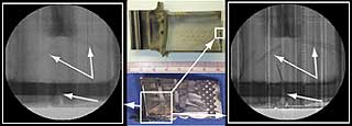
A Better Look at Fine DetailsA new form of neutron radiography that produces greatly enhanced images of fine structural details in test samples with relatively low levels of radiation has been demonstrated by researchers from NIST, the University of Melbourne, and the University of Missouri at Columbia. Conventional radiography, using either X-rays or neutrons, works by detecting the absorption of the radiation as it passes through different materials. For example, the radiograph shows the “shadows” cast by tumors (X-rays) or cracks in jet engine turbine blades (neutrons). But if two materials have very similar absorption characteristics or the feature under inspection is very small, then radiographs often show very little detail. In recent years, researchers have explored a more subtle effect called phase-sensitive imaging. As radiation passes through a specimen, the phase of the wave can shift at the boundary between materials of two different densities, just as light diffracts when passing through a glass of water. Because the phase-shift effect is often much stronger than the absorption effect, images based on the phase differences of the emerging waves can show much greater detail—particularly of boundaries or edges—with relatively smaller doses of radiation. The enhancement can be seen in the “before and after” images of the wasp and turbine blade below. Phase-contrast X-ray images have been studied for several years, and the dramatic images of tissue specimens clearly show fine details. But the experiments at NIST are the first to demonstrate the same phenomenon—and achieve equally dramatic image enhancement—using neutron beams, which have broad industrial applications in materials research.
Contact: Muhammad Arif, (301) 975-6303.
|
||
|
The same digital technology that fuels computers is coming to Hollywood in the form of digital cinema, which has replaced film in several theaters nationally. Digital cinema is billed as offering improved picture quality as well as savings in distribution costs because digital files can be transmitted by satellite or other means more cost-effectively than film can be printed and shipped. A recent conference at NIST on standards and interoperability issues in digital cinema attracted more than 240 participants and exhibitors, including major studios and computer makers. Participants identified a need for measurements to characterize the performance of electronic projectors and other system components, and to support open standards. Standards also are needed for the exchange, storage, and manifestation of digital content. The area of trust management–-digital rights management plus computer security—is viewed by industry as an important opportunity for NIST involvement. Contact: Victor McCrary, (301) 975-4321. Turning Seaweed into a Scientific Tool The wind resistance
of houses cannot be tested in traditional wind tunnels, which are
too small to hold a house. So where else can researchers find propellers
powerful enough to do the job? A machine too small to be seen with the naked eye has been invented by NIST researchers, who recently received a microsystems patent for the achievement. The patent covers a radically new way to make devices called accelerometers by combining new and existing technologies. Accelerometers have a variety of uses, such as detecting the sudden changes that set off air bags in car accidents or satellite tracking of acceleration and direction of cars. In the NIST process, integrated circuit technology widely used in the semiconductor industry is combined with a microscopic heater (also invented in NIST laboratories). Acceleration affects the convection process of gases, creating minuscule differences in temperature on both sides of the microheater. Sensors built into the chip then detect the temperature differences. The NIST patent is one in a series awarded for MicroElectroMechanical Systems, or MEMS. Contact: Michael Gaitan, (301) 975-2070.
|
||
Virtual Cement Laboratory—A new NIST/industry consortium has formed a Virtual Cement and Concrete Testing Laboratory, which is intended to expedite research and development by, for example, reducing the number of physical tests required to develop new, optimized cement-based materials. The virtual laboratory will include simulations of cement hydration, concrete structure, elastic properties, diffusion properties, permeability, and mortar and concrete rheology. Information on the consortium can be found at http://www.bfrl.nist.gov/862/vcctl, and Version 1.0 of the virtual laboratory is available at http://vcctl.cbt.nist.gov. Contact: Dale Bentz, (301) 975-5865. Combating Vehicle Fires-In research funded by General Motors, NIST is investigating the effectiveness of various fire suppressants in simulated post-collision vehicle fires. Among the results, NIST has found that on-board suppression systems will not extinguish all possible underbody and engine compartment fires. An emerging fire suppression system based on air bag technology and that burns a solid propellant was the most effective type tested in the full-scale engine compartment scenario. Contact: Anthony Hamins, (301) 975-6598. Non-linear Network Analysis—A new NIST facility has been established to develop advanced analysis and characterization methods for nonlinear radio-frequency and microwave electronics used in commercial wireless communications. The facility is used to investigate new metrology and modeling issues facing instrument designers, and is now being applied to laboratory intercomparisons and the development of new measurement-based circuit models. The core instrument is a nonlinear network measurement system, one of only seven in the world and the only one located in an open research environment in the Americas. Contact: Donald DeGroot, (303) 497-7212.
|
||
About Technology at a Glance:NIST is an agency of the US Department of Commerce's Technology Administration. NIST promotes US economic growth by working with industry to develop and apply technology, measurements, and standards. Technology at a Glance is produced by Public and Business Affairs, NIST, 100 Bureau Dr., Stop 3460, Gaithersburg, Md. 20899-3460. Any mention of commercial products is for information only; it does not imply recommendation or endorsement by NIST. Technology at a Glance Editor: Gail Porter, (301) 975-3392, email: gail.porter@nist.gov. For patent information, call (301) 975-3084. Technology at a Glance Archive Files
|


 The
progressive merging of optics and electronics technologies took a
step forward recently when Digital Optics Corp. (Charlotte, N.C.)
announced the successful completion of its
The
progressive merging of optics and electronics technologies took a
step forward recently when Digital Optics Corp. (Charlotte, N.C.)
announced the successful completion of its 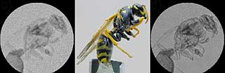
 With
500 kilograms of freeze-dried seaweed that originated off the shores
of Ireland, NIST plans to help the international community monitor
for radioactive contamination from Russian nuclear submarines that
were discarded in the Arctic Ocean. Seaweed is a key oceanic “sink”
for long-lived radioactive elements (e.g., radium, uranium), but there
is currently no
With
500 kilograms of freeze-dried seaweed that originated off the shores
of Ireland, NIST plans to help the international community monitor
for radioactive contamination from Russian nuclear submarines that
were discarded in the Arctic Ocean. Seaweed is a key oceanic “sink”
for long-lived radioactive elements (e.g., radium, uranium), but there
is currently no  Hercules
C-130 turboprop aircraft, of course. Tests planned in Lubbock, Texas,
will use propeller blasts from C-130s to subject instrument-laden
test homes to three sustained wind levels, one comparable to that
of a hurricane. NIST, Texas Tech University, the Department of Energy’s
Oak Ridge National Laboratory, and the Texas Air National Guard are
participating in the project. The researchers will make detailed measurements
of air flow properties, aerodynamic loads on selected points of the
buildings’ envelopes, and various features of the building response,
and also assess energy performance. Data analysis should yield realistic
computer models that can tell homebuilders and manufacturers the actual
wind resistance of different types of residential buildings under
any realistic wind condition. Contact:
Hercules
C-130 turboprop aircraft, of course. Tests planned in Lubbock, Texas,
will use propeller blasts from C-130s to subject instrument-laden
test homes to three sustained wind levels, one comparable to that
of a hurricane. NIST, Texas Tech University, the Department of Energy’s
Oak Ridge National Laboratory, and the Texas Air National Guard are
participating in the project. The researchers will make detailed measurements
of air flow properties, aerodynamic loads on selected points of the
buildings’ envelopes, and various features of the building response,
and also assess energy performance. Data analysis should yield realistic
computer models that can tell homebuilders and manufacturers the actual
wind resistance of different types of residential buildings under
any realistic wind condition. Contact: