|
|
||||||||||||||||||
|
|
The semiconductor and micro/nano-electronics industry plays a vital role in the continued growth of the US economy and national security. Since 1991, the Advanced Technology Program (ATP) of the National Institute of Standards and Technology (NIST), Technology Administration, U.S. Department of Commerce, has funded path-breaking new technologies of importance to this industry and the infrastructure upon which it depends. This report provides a historical review of ATP’s investments in technologies of importance to this industry. Characteristics of the Semiconductor and
|
||||||||||||||||||||||||||||||||||||||||||||||||||||||||||||||||||||||||||||||||||||||||||||||||||||||||||||||||||||||||||||||||||||||||||||||||||||||||||||||||||||||||||||||||||||||||||||||||||||||||||
| Total R&D Funded | $466.9 million |
Total Participants |
215 Entities |
ATP |
$229.9 million |
Small Companies |
75 |
Industry Cost-Share |
$237.0 million |
Medium Companies |
37 |
|
|
Large Companies |
59 |
Total Awards |
63 projects |
Not for Profit Organization |
6 |
Single Applicant |
40 projects |
Universities |
32 |
Joint Venture |
23 projects |
Federal Laboratories |
6 |
Table 2 below indicates the funding distribution among states, based on the location of the lead company for the award. The funding distribution shown does not reflect the actual funds that each state has received as projects distribute funds to several subordinate JV partners and subcontractors that may be located in other states.
Table 2
Semiconductor and Micro/Nano-Electronics Awards and Funding Among States
State |
AWARDS |
FUNDING* |
|||
|---|---|---|---|---|---|
Total |
Joint |
Single |
ATP |
Company Share $M |
|
CALIFORNIA |
18 |
6 |
12 |
$73.38 |
$83.31 |
COLORADO |
1 |
0 |
1 |
$1.99 |
$1.00 |
CONNECTICUT |
1 |
0 |
1 |
$1.71 |
$2.06 |
FLORIDA |
2 |
0 |
2 |
$3.86 |
$1.24 |
ILLINOIS |
2 |
2 |
0 |
$11.87 |
$12.48 |
KANSAS |
1 |
0 |
1 |
$2.00 |
$0.31 |
MARYLAND |
1 |
0 |
1 |
$1.97 |
$1.41 |
MASSACHUSETTS |
5 |
1 |
4 |
$9.93 |
$7.63 |
MICHIGAN |
5 |
4 |
1 |
$38.70 |
$40.58 |
MINNESOTA |
4 |
0 |
4 |
$6.25 |
$5.57 |
MISSISSIPPI |
1 |
0 |
1 |
$1.78 |
$0.76 |
MISSOURI |
1 |
0 |
1 |
$2.00 |
$1.50 |
NEW JERSEY |
3 |
2 |
1 |
$10.59 |
$12.19 |
NEW MEXICO |
1 |
0 |
1 |
$1.83 |
$.93 |
NEW YORK |
5 |
2 |
3 |
$8.81 |
$9.04 |
NORTH CAROLINA |
1 |
0 |
1 |
$1.96 |
$0.43 |
OREGON |
2 |
0 |
2 |
$3.58 |
$4.10 |
PENNSYLVANIA |
1 |
1 |
0 |
$2.94 |
$3.59 |
TEXAS |
7 |
4 |
3 |
$37.60 |
$40.60 |
VIRGINIA |
1 |
0 |
1 |
$1.99 |
$1.51 |
TOTAL |
63 |
22 |
41 |
$224.74 |
$230.24 |
* Funding amounts are a reflection of the state of residence of each award lead company. This table does not indicate the final distribution of funds to states based on the state of residences of JV partners, sub-contractors, universities, or consultants.
Electronics Manufacturing
Innovation lies at the heart of U.S. manufacturing leadership and success. Manufacturing advances create more efficient processes and higher quality products to meet consumer demands and customer service expectations. Electronics manufacturers strive to make improvements in manufacturing technologies to reduce cost and lead times. According to the National Association of Manufacturers (NAM):
ATP has co-funded 23 awards and stimulated approximately $184 million of total industry-based R&D with direct impact in semiconductor and electronics manufacturing. Of this approximately $92 million has come from ATP industry cost-shares each.
In 1998, ATP conducted a focused program competition on ‘Microelectronics Manufacturing Infrastructure’.7 The aim of this program was to help industry develop and improve technologies for microelectronics manufacturing integration, across suppliers and users, from chip to package to board. The objective was to enable world-class competitive electronic product manufacturing through product-driven industrial integration. Thus, the program intended to build manufacturing strengths within U.S. infrastructure companies, improve their capabilities, and improve the competitiveness of themselves, their customers, and the U.S. electronics industry as a whole.
Examples of ATP awards that illustrate innovations in electronics manufacturing include:
|
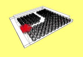
Intelligent Control of the Semiconductor Patterning Process
|
Distributed Factory System Framework Participant: Consilium Inc. |
Nanotechnology for Nano-Electronics
Nanotechnology is the understanding and control of matter at dimensions of roughly 1 to 100 nanometers, where unique phenomena enable novel applications.8 Novel and differentiating properties and functions of nanomaterials and nano-scale devices arise at this critical length scale of matter. Nanotechnology R&D seeks to:
ATP has co-funded 11 awards and stimulated approximately $112 million of total industry-based R&D with direct impact in nanotechnology for nano-electronics. Of this approximately $58 million has come from ATP with approximately $56 million of cost-share from industry.
Examples of ATP awards that illustrate innovations in nanotechnology for nano-electronics include:
Participant: Micro Magnetics Inc. |
Nano-Imprint Lithography Infrastructure for Low Cost Replication at the 65 nm Node and Beyond
|
The International Technology Roadmap for Semiconductors (ITRS), first produced in 1992 by the Semiconductor Industry Association as the National Technology Roadmap for Semiconductors, and now produced by the global semiconductor industry, is an assessment of the semiconductor industry’s technology requirements. The document, revised every 2 years, summarizes the technology trends and identifies the technical challenges that the industry will have to overcome to continuously deliver increased functionality at lower costs. The historical trend of reducing cost per function for electronics products - approximately 25-29 % per year – is viewed essential for the industry to realize continued market growth and further productivity increases across the economy.
Today, the ITRS represents an industry-wide view of R&D needs over the next 15-year period. Industry challenges within the 2005 ITRS are organized across specific technical and cross-cut areas.9
For the purpose of this report, the 63 ATP awards in semiconductor and micro/nano-electronics have been analyzed and distributed among nine technical categories that generally correspond to the eleven technical and four crosscut areas of the 2005 ITRS.
They are:
Distribution of ATP Awards in ITRS Technologies
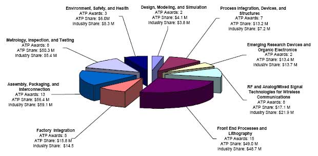
The projects are a reflection of industry’s pressing concerns and do not reflect any prioritization by ATP to any technical or crosscut area. The remainder of this report provides information for each technical category including examples of ATP co-funded awards. Appendix C shows all the ATP awards in these nine technical categories.
1. Front End Processes and Lithography
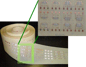
ATP has co-funded 16 awards and stimulated approximately $98 million of total industry-based R&D with direct impact in front end processes and lithography. Of this approximately $49 million has come from ATP with approximately $48.7 million of cost-share from industry.
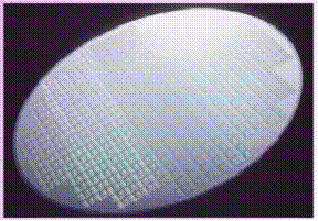
Technologies related to the fabrication of ICs on the semiconductor wafer are included within this category. The wafer diameters have increased from 200 nm to 300 nm, and are projected to go to 450 nm. At the same time the dimensions of the IC’s are shrinking.
Advances in wafer processing and lithography have major impacts on reducing IC dimensions, the cost of manufacturing, and overall reliability. These factors in turn have a direct impact on the performance and cost of products made using ICs. Challenges in this area include: new gate materials and processes; control of critical dimensions; scaling down of CMOS; control of surface interface properties; and new lithography and mask fabrication technologies.
ATP co-funded projects have created advancements in improved processing technologies, process integration, and new lithography technologies for CMOS manufacturing.
Examples of ATP awards that illustrate innovations in front end processes and lithography include:
Participant: Multibeam Systems Inc. |
Early Prototype Non-Gallium Ion Beam for Lithography and Wafer Manufacturing |
Gas-Cluster Ion-Beam Manufacturing Tool for Next-Generation Semiconductor Devices
|
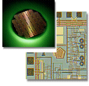
2. Assembly and Packaging
ATP has co-funded 13 awards and stimulated approximately $103 million of total industry-based R&D with direct impact in assembly, packaging, and interconnect. Of this approximately $50 million has come from ATP with approximately $53 million of cost-share from industry.
Technologies related to the interface between the IC and the electronics system are included within this category. Package design and fabrication is a very important part of the system and addresses issues related to materials, processes, and design. Embedded passive components are required for smaller smaller dimensions, reduced costs, and improved reliability.
Examples of ATP awards that illustrate innovations in assembly, packaging and interconnection include:
|
Advanced Embedded Passives Technology
|
Wafer-Scale Applied Reworkable Fluxing Underfill for Direct Chip Attach
|
Ultra-Low Dielectric Constant Materials for Integrated Circuit Participants:
|
3. Metrology, Inspection, and Testing
ATP has co-funded eight awards and stimulated approximately $106 million of total industry-based R&D with direct impact in metrology, inspection, and testing. Of this approximately $50 million has come from ATP with approximately $53 million of cost-share from industry.
U.S. manufacturers require a wide range of tools for inspecting and measuring their output for quality and performance. Metrology is essential for development and improvement of new materials, processes, and tools for manufacturing. Inspection of wafers and masks plays a critical role in defect reduction, yield improvement, and cost reduction.
As devices become smaller, the need for defect inspection becomes more and more critical. The need for R&D is in improving sensitivities, ability to detect smaller defects, and in inspection of high-aspect-ratio structures.
Examples of ATP awards that illustrate innovations in metrology, inspection, and testing include:
|
Micro-Contact Springs for High-Performance Probing and Packaging Participants:
|
Intelligent Mask Inspection System for Next-Generation Lithography Participants:
|
4. Environment, Safety, and Health
ATP has co-funded four awards and stimulated approximately $13 million of total industry-based R&D with direct impact in environment, safety, and health. Of this approximately $8 million has come from ATP with approximately $6 million of cost-share from industry.
Reducing the use of chemicals is one of the key issues in making the semiconductor fabrication process safer and more environmentally friendly. The semiconductor industry addresses environmental issues in various ways including development of alternatives to hazardous chemicals, reduction in emission of pollutants, conservation of natural resources, and substituting environmentally benign solvents in manufacturing. Some key challenges in environmentally benign semiconductor manufacturing include:
Examples of ATP awards that illustrate innovations in environment, safety and health include:
 |
ACIM "Point*Suns": Concentrating Energy Through Silent Sound and Clean Water |
|
Contact Planarization for Microlithographic Processes |
5. Design, Modeling, and Simulation
ATP has co-funded two awards and stimulated approximately $13 million of total industry-based R&D with direct impact in design, modeling, and simulation. Of this approximately $7 million has come from ATP with approximately $6 million of cost-share from industry.
This category addresses a critical aspect in advancement of miniaturization in the semiconductor industry. Errors in design lead to lower yields and reduced reliability of ICs and system-on-chip (SoC). Some matters important for further miniaturization include: accurate designs, identification and correction of design errors, designing probes for testing, and efficiently testing for defects. Miniaturization leads to reduced costs of electronic products and increases the scope of applications.
Examples of ATP awards that illustrate innovations in design, modeling and simulation include:
Reconfigurable Infrastructure Platform for Systems-on-Chips |
Membrane Probes for Wafer, Package, and Substrate Testing |
6. Process Integration, Devices, and Structures
ATP has co-funded six awards and stimulated approximately $17 million of total industry-based R&D with direct impact in process integration, devices, and structures. Of this approximately $11 million has come from ATP with approximately $6 million of cost-share from industry.
Technologies that affect the process flow and manufacturability associated with new ways of integrating active devices with different structures or materials; integrate different types of active devices; integrate active devices with on-chip interconnects; or that integrate different processing technologies are included within this category. Such types of integration enable the use of different materials and technologies, each having unique advantages and performance characteristics, for specific applications.
Examples of ATP awards that illustrate innovations in process integration, devices and structures include:
|
Nanophotonic Integrated Circuits for Telecommunications and Computing |
PowerFlow: Next-Generation Intellectual Property Technology for System-on-a-Chip Designs |
7. Emerging Research Devices
ATP has co-funded three awards and stimulated approximately $40 million of total industry-based R&D with direct impact in emerging research devices and organic electronics. Of this approximately $20 million has come from ATP with approximately $20 million of cost-share from industry.
Conventional semiconductor materials and processes technologies are not very well suited for large area electronic devices such as displays because of size and cost issues. Flexible electronics, organic semiconductor materials and associated manufacturing technologies offer potential solution to these hurdles.
Examples of ATP awards that illustrate innovations in emerging research devices include:
Printed Organic ASICs: A Disruptive Technology Participants:
|
Nanoengineered Thermal Interfaces Enabling Next Generation Microelectronics Participants:
|
8. RF and Analog/Mixed Signal Technologies for Wireless Communication
ATP has co-funded six awards and stimulated approximately $27 million of total industry-based R&D with direct impact in RF and Analog/Mixed-signal technologies for wireless communications. Of this approximately $13 million has come from ATP with approximately $14 million of cost-share from industry.
Wireless technologies play a critical role in emergency response, military applications, transportation, and manufacturing. Cost and performance determine how widely the technology will be applied. Advancements in wireless telecommunications require development in materials, design, and manufacturing technologies to reduce cost and improve performance.
Examples of ATP awards that illustrate innovations in RF and analog mixed signal technologies for wireless communications include:
Rapid and Comprehensive Development of Advanced Dielectric Materials for Wireless Applications |
Advanced Receiver Front-end Technology for 4G Wireless Systems |
9. Factory Integration
ATP has co-funded five awards and stimulated approximately $30.3 million of total industry-based R&D with direct impact in factory integration. Of this approximately $16 million has come from ATP with approximately $14 million of cost-share from industry.
Technologies important for improved factory productivity are included within this category. Some challenges include: technologies for operational effectiveness, integrated factory level control system, process and equipment control, manufacturing information and execution systems, data handling, and automated control systems. Overcoming these challenges enables the industry to increase equipment utilization, decrease cycle time, improve yields, and lower cost of production.
Examples of ATP awards that illustrate innovations in factory integration include:
eManufacturing Security Framework to Improve Semiconductor Manufacturing Productivity Participants:
|
Intelligent Equipment for Semiconductor Manufacturing |
The Advanced Technology Program (ATP) at the National Institute of Standards and Technology has co-funded, along with industry participants, high-risk innovative research that has a significant impact on the nation’s technology base, competitiveness and economic welfare of the nation. Since 1991, ATP has funded 63 awards, across 20 states, involving 215 entities, in innovative technologies important to semiconductor and micro/nano-electronics. This amounts to approximately $467 million of total, industry-based R&D. A large number of these ATP awards have collaborations between companies, universities, and national laboratories, with 23 out of the 63 awards being joint ventures between involving at least two or more companies. Universities have also played a critical role in ATP semiconductor and micro/nano-electronics awards as joint venture partners, subcontractors, or in transfer of technology from university research to commercial applications. A total of 32 instances of university participation, or on average one university for every two ATP awards, have occurred in this technology area.
Contact Information
For information about the Advanced Technology Program, contact:
Telephone: (800) ATP‑FUND (800‑287‑3863)
Internet: http://www.atp.nist.gov .
E-mail: atp@nist.gov
FAX: (301) 926‑9524
Mail: 100 Bureau Drive, MS4700
National Institute of Standards and Technology
Gaithersburg, MD 20899‑4700
For further information on these and other ATP funded projects, visit the ATP website at www.atp.nist.gov.
___________________
1. SEMI presentation by Lara Chamness, February 22, 2006, ‘2005: A year in review for the semiconductor equipment and materials market and trends moving forward’
http://content.semi.org/cms/groups/public/documents/newsresources/p037643.pdf.
2. A nanometer is one-billionth of a meter (10-9 m). The width of an average human hair is approximately 100,000 times larger than one nanometer.
3. Semiconductor Industry Association 2006 annual report http://www.sia-online.org.
4. Semiconductor Industry Association, Choose to Compete: Semiconductors and America’s innovation leadership http://www.choosetocompete.org/us_chip_industry.html .
5. Competing for the Future: A Historical Review of NIST ATP Investments in Photonics and Optical Technologies
http://www.atp.nist.gov/iteo/elec_photon.htm.
6. National Association of Manufacturers, ‘Why Manufacturing is Essential http://www.nam.org/s_nam/sec.asp?CID=201648&DID=230169.
7. Microelectronics Manufacturing Infrastructure (MMI), 1998 Focused Program Paper http://www.atp.nist.gov/atp/97wpm212.htm.
8. http://www.nano.gov/html/facts/whatIsNano.html
9. ITRS, 2005 Edition, http://www.itrs.net/Common/2005ITRS/Home2005.htm
10. NSF/SRC Engineering Research Center for Environmentally Benign Semiconductor Manufacturing
http://www.erc-assoc.org/factsheets/h/html/erc_h.htm
Go to Appendix A.
Date created: July 11, 2006
Last updated:
August 29, 2006
| ATP
website comments: webmaster-atp@nist.gov / Technical
ATP inquiries: InfoCoord.ATP@nist.gov NIST is an agency of the U.S. Commerce Department Privacy policy / Security Notice / Accessibility Statement / Disclaimer / Freedom of Information Act (FOIA) / No Fear Act Policy / NIST Information Quallity Standards / ExpectMore.gov (performance of federal programs) |

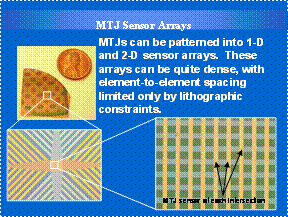 Spintronics-Based High-Resolution, Non-Invasive, and Ultrafast Metrology for the Semiconductor Industry
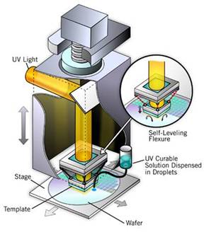
 Development and Demonstration of a Multiple, High-Current-Density Shaped E-Beam Column with Independent Vector Beam Placement