| September 3, 2008

[NIST Tech Beat Search] [Credits] [NIST Tech Beat Archives] [Media Contacts] [Subscription Information]

Bottoms Up: Better Organic Semiconductors for Printable Electronics
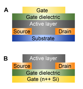 |
Restacking organic semiconductors: An improved formulation for a polymer blend semiconductor causes key semiconducting molecules to migrate to the bottom of the active layer, allowing chip designers to replace top-gated structures (a) with more easily manufactured bottom-gate, bottom-contact devices (b).
Credit: Yoon, SNU/Talbott, NIST
View hi-resolution image |
Researchers from the National Institute of Standards and Technology (NIST) and Seoul National University (SNU) have learned how to tweak a new class of polymer-based semiconductors to better control the location and alignment of the components of the blend. Their recent results—how to move the top to the bottom—could enable the design of practical, large-scale manufacturing techniques for a wide range of printable, flexible electronic displays and other devices.*
Organic semiconductors—novel carbon-based molecules that have similar electrical properties to more conventional semiconducting materials like silicon and germanium—are a hot research topic because practical, high-performance organic semiconductors would open up whole new categories of futuristic electronic devices. Think of tabloid-sized “digital paper” that you could fold up into your pocket or huge sheets of photovoltaic cells that are dirt cheap because they’re manufactured by—basically—ink-jet printing.
The problem is performance. Small organic molecules have been developed with key electrical parameters close to the benchmark set by amorphous silicon semiconductors, but they are very difficult to deposit in a stable, uniform film—a key manufacturing requirement. Larger molecule polymer semiconductors, on the other hand, make excellent thin films but have at best limited semiconductor properties. A patent from British researchers in 2005 offered a promising compromise: blend the small semiconductor molecules in with the polymer. This works surprisingly well, but with an asterisk. Tests showed that actual devices, field effect transistors, made with the blend only worked well in a so-called “top-gated” structure. The critical active part of the film was on the top, and the switching part of the device (the “gate”) had to be layered on top of that, a process difficult or impossible to do on a large scale without destroying the fragile film.
Working at NIST’s Center for Neutron Research, the SNU/NIST research team used a neutron imaging technique that allowed them to observe, with nanometer resolution, how the distribution of small organic semiconductor molecules embedded in polymer films changed with depth—the films are less than 100 nanometers thick. In the thin films originally described by the patent, the bulk of the semiconductor molecules end up at the top of the film, as suspected. However, when the SNU/NIST research team substituted a polymer with significantly higher molecular mass, something interesting happened. The organic semiconductor small molecules distributed themselves evenly at the top and bottom of the film. Having an active region of the film on the bottom is key for large-scale manufacturing because it means the rest of the device—gate, source, drain—can be laid down first and the delicate film layer added last.
In addition, they report, the optimized blend of polymer and organic semiconductor actually has better performance characteristics than the organic semiconductor on its own.
* J. Kang, N. Shin, D.Y. Jang, V.M. Prabhu and D.Y. Yoon. Structure and properties of small molecule-polymer blend semiconductors for organic thin film transistors. Journal of the American Chemical Society, Published on the Web Aug. 23, 2008.
Media Contact: Michael Baum, michael.baum@nist.gov, (301) 975-2763 
NIST Studies How New Helium Ion Microscope Measures Up
 |
In-depth look: An image of gold atoms on tin from a state-of-the-art scanning electron microscope (left) has relatively poor depth of field–only parts of the image are in sharp focus. By contrast, the entire image from a helium ion microscope image (right) is sharp and clear. NIST researchers are studying helium ion microscopes to improve measurements at the nanoscale that are important to the semiconductor and nanomanufacturing industries.
Credit: NIST
View hi-resolution image |
Just as test pilots push planes to explore their limits, researchers at the National Institute of Standards and Technology (NIST) are probing the newest microscope technology to further improve measurement accuracy at the nanoscale. Better nanoscale measurements are critical for setting standards and improving production in the semiconductor and nanomanufacturing industries.
This new microscope technology uses helium ions to generate the signal used to image extremely small objects, a technique analogous to the scanning electron microscope, which was first introduced commercially in the 1960s. Paradoxically, although helium ions are far larger than electrons, they can provide higher resolution images with higher contrast. The depth of field is much better with the new technology too, so more of the image is in focus. “It is the physics,” explains Andras Vladar, SEM project leader in NIST’s Nanoscale-Metrology Group. “Ions have larger mass and shorter wavelength than electrons, so they can be better for imaging.” The images, he says, appear almost three-dimensional, revealing details smaller than a nanometer—the distance spanned by only three atoms in the silicon crystal.
NIST is working to understand the imaging mechanisms of this new technology. The clearest advantage of the helium ion microscope is that the images show the actual edge of a sample better than the SEM, which is critical in precision manufacturing. “Meeting critical dimensions by knowing where an edge is in high-tech manufacturing can mean the difference of hundreds of dollars per piece,” explains Michael Postek, chief of the NIST Precision Engineering Division and the nanomanufacturing program manager. Semiconductor manufacturers have multi-million dollar scanning electron microscopes all along their production lines to help control their microchip manufacturing processes.
NIST received the first-ever commercial helium ion microscope, called Orion, from Carl Zeiss, Inc., last summer as part of a cooperative research and development agreement (CRADA). Researchers are test-piloting it in NIST’s Advanced Measurement Laboratory (AML), one of the most environmentally stable research facilities in the world. Carefully controlled for vibration, humidity and temperature changes, AML labs are optimal sites to test new microscope technology, say the researchers. “What we are learning,” explains Postek, “goes directly back to the manufacturers to improve their products, which allows NIST and industry to obtain the most precise measurements possible. We are transferring NIST technology and sharing our research with the semiconductor industry trade organization, SEMATECH.”
One such NIST contribution is “fast imaging,” a technique Vladar developed to obtain sharper images. A combination of vibrations at the nanoscale and taking images at high resolutions left certain images fuzzy, similar to what happens when taking a picture of a moving baby with a slow shutter speed. Instead of collecting the signal slowly and getting a fuzzy image, the NIST technique collects many images as fast as possible and merges them using a clever algorithm to reduce the fuzziness and result in a much sharper image.
Zeiss has recently replaced the original Orion with the first-ever Orion Plus, which incorporates many of NIST’s suggestions in its design, including an improved cooling system for the helium source for improved imaging.
Media Contact: Evelyn Brown, evelyn.brown@nist.gov, (301) 975-5661
NIST Releases WTC 7 Investigation Report for Public Comment
The fall of the 47-story World Trade Center building 7 (WTC 7) in New York City late in the afternoon of Sept. 11, 2001, was primarily due to fires, the National Institute of Standards and Technology (NIST) announced on August 21 following an extensive, three-year scientific and technical building and fire safety investigation. This was the first known instance of fire causing the total collapse of a tall building, the agency stated as it released for public comment its WTC investigation report and 13 recommendations for improving building and fire safety.
“Our study found that the fires in WTC 7, which were uncontrolled but otherwise similar to fires experienced in other tall buildings, caused an extraordinary event,” said NIST WTC Lead Investigator Shyam Sunder. “Heating of floor beams and girders caused a critical support column to fail, initiating a fire-induced progressive collapse that brought the building down.”
“Video and photographic evidence combined with detailed computer simulations show that neither explosives nor fuel oil fires played a role in the collapse of WTC 7,” Sunder said. The NIST investigation team also determined that other elements of the building’s construction—namely trusses, girders and cantilever overhangs that were used to transfer loads from the building superstructure to the columns of the electric substation (over which WTC 7 was constructed) and foundation below—did not play a significant role in the collapse.
According to the report, a key factor leading to the eventual collapse of WTC 7 was thermal expansion of long-span floor systems at temperatures “hundreds of degrees below those typically considered in current practice for fire resistance ratings.” WTC 7 used a structural system design in widespread use.
Citing its one new recommendation (the other 12 are reiterated from the previously completed investigation of the World Trade Center towers, WTC 1 and 2), the NIST investigation team said that “while the partial or total collapse of a tall building due to fires is a rare event, we strongly urge building owners, operators and designers to evaluate buildings to ensure the adequate fire performance of the structural system. Of particular concern are the effects of thermal expansion in buildings with one or more of the following features: long-span floor systems, connections not designed for thermal effects, asymmetric floor framing and/or composite floor systems.” Engineers, the team said, should be able to design cost-effective fixes to address any areas of concern identified by such evaluations.
NIST welcomes comments on the draft report and recommendations received by noon Eastern Daylight Time on Sept.15, 2008. Instructions for submitting comments—as well as links to the complete text of the draft WTC 7 investigation report, archived videos of the Aug. 21 press briefing and an Aug. 26 technical briefing, a video describing the WTC 7 investigation findings, and other materials—may be accessed at http://wtc.nist.gov.
Media Contact: Michael E. Newman, michael.newman@nist.gov, (301) 975-3025
New NIST Publication Series Addresses Design of Earthquake-Resistant Structures
Where can you find some of the latest insights in designing earthquake-resistant buildings joined together with current information on building codes? As part of its support for the National Earthquake Hazards Reduction Program (NEHRP), the National Institute of Standards and Technology (NIST) has released a publication that provides guidelines for designing a special type of structural frame used in regions with high seismic activity.*
The new NIST publication is the first of a special series of “techbriefs” intended to address topics of interest to earthquake professionals in the design and construction industries. NIST anticipates issuing one to three such briefs each year.
Technical Brief No. 1 describes the design of concrete-reinforced “special moment frames,” structural systems that consist of beams and columns with connections that transmit bending forces (moments) from the beams to columns and vice versa. The term “special” is used in the structural engineering community and model building codes to denote systems that are designed and detailed for use in geographic areas where seismic effects can be large.
The document provides design guidance by combining what is required by building codes with knowledge gained in recent research and design practice. The Applied Technology Council (ATC) and the Consortium of Universities for Research in Earthquake Engineering (CUREE) are partners in the joint venture, with which NIST has a five-year research contract.
Technical Brief No. 1 is available in downloadable electronic form at the NEHRP Web site (www.nehrp.gov), as well as the Web sites for ATC (www.atcouncil.org) and CUREE (www.curee.org).
The techbrief concept was originally proposed by a group of nationally recognized earthquake professionals in 2003 in ATC-57, The Missing Piece: Improving Seismic Design and Construction Practices. NIST anticipates producing a techbrief on seismic design of steel-based special moment frames in 2009.
* J.P. Moehle, J.D. Hooper and C.D. Lubke. Seismic Design of Reinforced Concrete Special Moment Frames: A Guide for Practicing Engineers. NIST GCR 8-917-1, NEHRP Seismic Design Technical Brief No.1. Available at www.nehrp.gov/pdf/nistgcr8-917-1.pdf.
Media Contact: Ben Stein, bstein@nist.gov, (301) 975-3097
Quick Links
NIST Physicist Wineland Awarded 2007 National Medal of Science
Physicist David J. Wineland of the National Institute of Standards and Technology (NIST) has been awarded the 2007 National Medal of Science.
Wineland, 64, was cited for “outstanding leadership in developing the science of laser cooling and manipulation of ions, with applications in extremely precise measurements and standards, quantum computing, and fundamental tests of quantum mechanics, and for his major impact on the international scientific community through training scientists and outstanding publications.” He is internationally recognized for developing the technique of using lasers to cool ions to near absolute zero, the coldest possible temperature. Wineland achieved the first demonstration of laser cooling in 1978 and has built on that breakthrough with 30 years of experiments in using trapped laser-cooled ions to test theories in quantum physics and demonstrate crucial applications such as new forms of computation.
The National Medal of Science honors individuals for pioneering scientific research in a range of fields, including physical, biological, mathematical, social, behavioral and engineering sciences, that enhances understanding of the world and leads to innovations and technologies that give the United States a global economic edge. The National Science Foundation administers the award, which was established by the Congress in 1959. The winners will be honored at a ceremony in Washington, D.C., on Sept. 29.
For more details, see “NIST Physicist David J. Wineland Awarded 2007 National Medal of Science.”
.
NIST To Host 4th Security Automation Conference and Workshop
From Sept. 22-25, 2008, the National Institute of Standards and Technology (NIST) will host a conference and accompanying workshops demonstrating the use of open standards to automate computer security tasks. The 4th annual 2008 Security Automation Conference and Workshop will take place at the NIST campus in Gaithersburg, Md. from Sept. 22-25, 2008, and is co-sponsored by NIST, the National Security Agency (NSA), the Defense Information Systems Agency, and the Department of Homeland Security.
The conference will contain the latest information on the computer-security specification known as the Security Content Automation Protocol (SCAP), which can be used to automate tasks needed to comply with federal directives such as the Federal Information Security Management Act (FISMA) and the Federal Desktop Core Configuration (FDCC). It will also showcase emerging topics such as digital rights management, virtualization, and situational awareness, in which data are collected in order to grasp a situation and predict its course.
This year’s workshops are being split into two tracks: management and technical. Keynote addresses will feature speakers from NSA and other organizations. Vendors will demonstrate SCAP-validated products.
General registration closes on Sept. 16. More information on the conference can be found at www.nist.gov/public_affairs/confpage/080923.htm
Biometric Consortium Conference 2008 Will Be Held Sept. 23-25
The Biometric Consortium Conference 2008, to be held in Tampa, Fla., Sept. 23-25, will focus on biometric technologies for homeland security, identity management, border crossing, electronic commerce and other applications. It will include two and a half days of presentations, seminars and panel discussions with the participation of internationally recognized experts in biometric technologies, system and application developers, IT business strategists, and government and commercial officers.
Workshops, sessions and panel discussions featuring more than 100 speakers will focus on the important role that biometrics can play in the identification and verification of individuals in government and commercial applications worldwide.
More than 1000 participants are expected to attend, including representatives from 60 federal, state and local agencies, 25 universities, the biometric industry, system integrators and users. Topics will include the recently published report from the National Science and Technology Council’s Task Force on Identity Management. Duane Blackburn, policy analyst from the White House’s Office of Science and Technology, will moderate a panel discussion on the report and deliver the opening address on government biometrics policy.
The conference is being co-sponsored by the National Institute of Standards and Technology, the National Security Agency, the Department of Homeland Security, the Department of Defense Biometric Task Force, the National Institute of Justice, the Office of Technology Strategy of the General Services Administration, the Department of Transportation’s Volpe Center and the Armed Forces Communications and Electronics Association.
For more information see the conference Web site: www.biometrics.org/BC2008.
Coming Soon! Baldrige Recipients Share Successes
Senior leaders from the five organizations selected for the 2007 Malcolm Baldrige National Quality Award, as well as representatives from past Award recipients, will share their best practices and results at one-day regional conferences on Sept. 16, 2008, in Denver, Colo., and Oct. 3, 2008, in New Orleans, La. Participants can network with the recipients and gather valuable tips on applying the Baldrige Criteria for Performance Excellence.
The 2007 Baldrige Award recipients—listed with their category—are:
- PRO-TEC Coating Co., Leipsic, Ohio (small business)
- Mercy Health System, Janesville, Wisc. (health care)
- Sharp HealthCare, San Diego, Calif. (health care)
- City of Coral Springs, Coral Springs, Fla. (nonprofit)
- U.S. Army Armament Research, Development and Engineering Center (ARDEC), Picatinny Arsenal, N.J. (nonprofit)
The Baldrige Award promotes excellence in organizational performance, recognizes the achievements and results of U.S. organizations, and publicizes successful performance strategies. The Award is not given for specific products or services. Since 1988, 72 organizations have received Baldrige Awards.
For more information on the regional conferences and to register online, go to www.baldrige.nist.gov/2008_Regionals/Regionals.htm. You also may contact the Baldrige Program at (301) 975-2036 or nqp@nist.gov.
|